Individuals often believe that purchasing high-quality service inevitably requires shelling out a sizable amount of money. It is undoubtedly true in a number of situations that you get what you pay for, particularly in the case of products with intricate cost-effective manufacturing processes like printed circuit boards (PCBs).
One would imagine that electronics manufacturing services will be expensive because they involve numerous phases, sophisticated technology, and expert labor. But, you don’t always need to spend a fortune to acquire a product that lives up to your expectations.
Surprisingly, there are methods to reduce expenses without sacrificing the quality of the PCB layouting and manufacturing process, even though it is true that these processes are inherently complicated.
This blog serves as a comprehensive guide, outlining nine practical steps to streamline your PCB production processes while maintaining quality and maximizing efficiency.
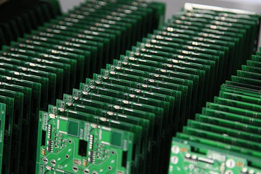
9 Steps to Cost-Effective PCB Manufacturing
1. Size of the PCB
Size matters, especially in the realm of PCB production. When designing your PCB, carefully consider its dimensions. Larger PCBs typically require more material and longer production times, consequently driving up costs. By optimizing the size of your PCBs without compromising functionality, you can significantly reduce production expenses. Moreover, smaller PCBs are often more space-efficient, allowing for higher yields per panel during assembly.
2. Consider the Size of the Panel
In addition to individual PCB size, it’s essential to factor in the size of the manufacturing panel. PCB contract manufacturing companies often utilize standardized panel sizes for efficiency. Designing your PCB layout to fit these standard panel dimensions can minimize waste and increase production throughput.
Efficient panel utilization not only reduces material costs but also optimizes the use of manufacturing equipment, ultimately enhancing overall efficiency. When it comes to design, the PCB with each part reserves a second source material, which will further avoid procurement accidents or high pricing.
3. More Layers = More Cost
When considering the design of a printed circuit board (PCB), weighing the benefits against the costs, particularly regarding the number of layers, is essential. While multi-layer PCBs undoubtedly offer enhanced functionality and performance, they also come with a higher price tag. This increase in cost is primarily due to the added complexity involved in the manufacturing process.
The PCB manufacturing process becomes more intricate with each additional layer added to the PCB board design. This complexity requires more materials, time, and resources to produce the board effectively. From the fabrication of the individual layers to the intricate process of laminating and bonding them together, every step adds to the overall production expenses.
Before opting for a multi-layer design, it’s crucial to carefully assess whether the added benefits justify the increased production costs. While multi-layer PCBs offer advantages such as improved signal integrity, reduced electromagnetic interference, and greater design flexibility, these benefits must be weighed against the financial implications.
4. Use the Largest Diameter Holes Possible
When designing PCBs, the size of drilled holes plays a crucial role in PCB manufacturing companies. Larger diameter holes are easier and faster to drill, reducing production time and minimizing tool wear.
Utilizing the largest diameter holes possible within your design constraints can streamline the drilling process and lower manufacturing costs. Additionally, larger holes provide greater tolerance for alignment errors during assembly, enhancing overall yield and reliability. Also, try to replace THT parts with more SMT parts and minimize the manual operation of the product. This will improve the automatic process and save costs, too.
5. Do Not Make the PCB Complex
Simplicity is critical to cost-effective electronic PCB manufacturing services. Complex designs with intricate features and tight tolerances increase production complexity and raise the risk of errors and defects.
Simplifying your PCB design by minimizing unnecessary components, reducing routing complexity, and optimizing layout efficiency can significantly lower production costs. Focus on functionality and reliability, avoiding unnecessary complexity that adds little value to the end product.
Your DFM(Design for Manufacturability) best practice will make a considerable difference as the DFM methodology differs from the bare PCB level, and the PCB assembly level will ensure the design is within the capability of PCB manufacturing and PCB assembly factories.
6. Let the Copper Line Be Thin
When designing a printed circuit board (PCB), it’s crucial to consider every element meticulously, including the thickness of copper traces. Copper traces serve as the pathways for conducting electrical signals throughout the PCB.
While these traces are indispensable for the board’s functionality, excessive copper thickness can lead to inflated production costs. Therefore, keeping the copper lines as thin as possible is prudent without sacrificing performance.
Thinner copper traces offer several advantages in PCB layout design. Firstly, they require less material, which translates to cost savings in production. With thinner traces, less copper is utilized, reducing the overall material expenditure. Additionally, thinner traces necessitate shorter etching times during the PCB manufacturing process. This saves time and lowers production costs associated with the etching process.
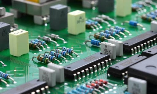
7. The Obvious: Use Quality Materials
Quality should never be compromised in the pursuit of cost savings. Using inferior materials may reduce upfront costs but can lead to reliability issues, performance degradation, and higher failure rates down the line. Partner with reputable PCB manufacturing companies that prioritize quality and reliability. Select materials that meet industry standards and specifications, ensuring optimal performance and longevity for your PCBs.
Another cost-effective practice in PCB manufacturing companies is to choose popular components that are reasonably priced and currently in a rising phase. This approach helps reduce expenses and simplifies the procurement process.
8. Understand the Drill-to-Copper Concept
The drill-to-copper concept refers to the relationship between drill size and copper pad size on a PCB. Properly optimizing this relationship can improve manufacturing efficiency and reduce costs. By matching drill sizes to copper pad diameters, you can minimize the amount of copper removed during drilling, resulting in faster drilling times and reduced material waste. Maintaining consistent drill-to-copper ratios across your PCB design also ensures uniformity and reliability in the manufacturing process.
Consistency in drill-to-copper ratios across the entire PCB design ensures uniformity and reliability throughout manufacturing. When the drill-to-copper ratios are consistent, it helps maintain uniformity in hole sizes and copper pad dimensions across the PCB.
This uniformity is essential for achieving reliable electrical connections and ensuring the PCB functions as intended.
9. Ensure Compliance, Assurance, and Conformance
Compliance with industry standards and regulations is non-negotiable in PCB manufacturing. Ensure that your designs adhere to relevant standards such as IPC (Association Connecting Electronics Industries) specifications to guarantee product reliability and compatibility. Work closely with your manufacturing partners to establish quality assurance processes and conduct thorough inspections throughout the production lifecycle.
Deviating from these standards can compromise the integrity of the PCB layout design and lead to performance issues or even product failure. Close collaboration between design teams and PCB manufacturing partners is essential to establish robust quality assurance processes.
Manufacturers bring invaluable expertise, offering insights into production techniques, material considerations, and testing methodologies.
Final Thoughts
In the dynamic landscape of electronics PCB manufacturing, achieving cost control and efficiency improvement is a continuous journey. Implementing the nine practical steps outlined in this guide can streamline your PCB production processes, reduce costs, and enhance overall efficiency. Collaborate with experienced PCB manufacturing companies that prioritize quality, reliability, and innovation to stay ahead in this competitive industry.
Remember, success in PCB manufacturing hinges on striking the right balance between cost optimization and quality assurance. With careful planning, strategic decision-making, and a commitment to excellence, you can navigate the complexities of PCB manufacturing and unlock new opportunities for growth and innovation in the electronics market.