In the world of electronics, where functionality, speed, and efficiency reign supreme, the layout of a Printed Circuit Board (PCB) holds unparalleled importance. It’s not an overstatement to say that the success of an electronic product hinges on the precision and thoughtfulness put into its Pcb layout. The intricate dance of traces, components, and signals on a PCB determines the device’s performance, reliability, and overall functionality. In this blog, we’ll delve into the world of PCB layout, exploring the critical steps, effective tips, and advanced techniques that engineers employ to achieve optimal PCB layout optimization. From the careful placement of components to the strategic routing of traces, every decision in the Pcb layout process contributes to the device’s performance prowess.
The Role of Pcb layout in Performance
Importance of Pcb layout
At the heart of every electronic device lies a PCB, a canvas of interconnected pathways that determine how signals flow and interact. A well-executed Pcb layout goes beyond aesthetics; it’s a meticulous choreography that influences signal integrity, noise levels, thermal management, and ultimately, the device’s overall performance. Whether it’s a smartphone, a medical device, or an industrial machine, the quality of the Pcb layout directly impacts the functionality of the end product.
Impact on Signal Integrity
Signal integrity is the holy grail of PCB design. It refers to how well a signal maintains its original waveform as it travels through the traces. Proper Pcb layout plays a pivotal role in preserving signal integrity. The length, width, and routing of traces directly affect signal propagation, quality, and susceptibility to noise. In high-speed designs, maintaining controlled impedance traces is paramount for preventing signal degradation and ensuring reliable data transmission.
Key Steps in Pcb layout for Performance
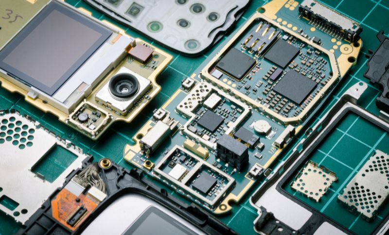
Component Placement
Component placement is the cornerstone of an efficient and high-performance Pcb layout. It’s where the architecture of your design takes shape, and careful consideration at this stage can greatly influence the success of your final product. The following aspects play a crucial role in optimizing component placement for maximum performance:
Strategic Signal Paths:
The proximity of components to one another can significantly impact signal paths. Grouping related components together minimizes trace lengths and reduces the chances of signal interference. Components that frequently communicate or share data should be positioned close to one another to reduce signal propagation delays.
Thermal Considerations:
Certain components generate more heat than others during operation. Placing heat-generating components near each other and providing ample space for effective heat dissipation is essential to prevent thermal issues. Components sensitive to temperature variations, such as precision oscillators, should be placed away from heat sources, ensuring a balanced thermal profile across the creating pcb.
Sensitivity to Noise:
Some components, especially analog and RF components, are highly sensitive to noise. Placing noisy components, like switching power supplies, away from these sensitive components helps minimize noise coupling. Additionally, ground planes or guard traces can be used to shield noise-sensitive components from unwanted interference, maintaining signal clarity in the creating pcb.
Simulation Tools:
The advancement of simulation tools empowers engineers to predict the impact of different component placements on signal integrity and thermal behavior. Tools like Electromagnetic Interference (EMI) simulation software can simulate the radiated emissions from components and traces, guiding designers to make informed placement decisions that optimize the creating pcb.
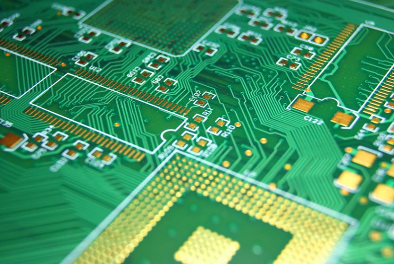
Traces and Routing
Once components are strategically placed, the next step is to lay down the traces that connect them. Effective trace routing ensures proper connectivity and plays a crucial role in maintaining signal integrity and reducing noise susceptibility. Here are key considerations for optimal trace routing in creating pcbs:
Signal Trace Lengths:
For signals traveling at high speeds, trace length matching becomes essential to prevent signal skew and timing mismatches. Techniques like length matching and phase tuning help ensure that critical signals arrive at their destinations simultaneously, preserving signal coherence within the creating pcb.
Avoiding Sharp Angles:
Sharp angles and abrupt turns in trace routing can lead to signal reflections and impedance mismatches. Gentle curves and rounded corners minimize the risk of signal degradation and electromagnetic interference, contributing to a reliable creating pcb.
Differential Pair Routing:
High-speed differential signals, commonly used in applications like USB, HDMI, and PCIe, require careful routing to maintain signal balance and prevent common-mode noise. Keeping the two traces of a differential pair close together and ensuring they have equal lengths is vital for noise reduction and optimal performance of the creating pcb.
Ground Planes and EMI Mitigation:
A solid ground plane beneath signal traces acts as a shield against electromagnetic interference (EMI). To minimize EMI, ground planes can be segmented to isolate different sections of the circuit, such as analog and digital domains, enhancing the overall EMI performance of the creating pcb.
Power Distribution and Grounding
The power distribution network (PDN) is the backbone of a PCB, ensuring that all components receive the necessary power supply. Effective power distribution and grounding strategies are essential to maintain stable voltage levels and reduce noise. Key considerations for power distribution and grounding in creating pcbs include:
Power Planes:
Multilayer PCBs often utilize power planes to provide a stable voltage supply to components. These planes act as reservoirs of power, preventing voltage droops during transient load changes. Careful partitioning of power planes and using multiple power layers can enhance the power distribution network, contributing to efficient power delivery throughout the creating pcb.
Decoupling Capacitors:
Placing decoupling capacitors close to power pins of ICs helps mitigate voltage fluctuations caused by sudden changes in current demand. These capacitors act as local energy reservoirs and stabilize the power supply, enhancing the stability of the creating pcb.
Separate Ground Domains:
The separation of ground domains is essential for preventing noise coupling between different sections of the circuit. Separating analog and digital ground domains helps minimize the interference generated by high-speed digital signals from affecting sensitive analog components, ensuring a clean ground reference in the creating pcb.
Tips and Techniques for Optimal Pcb layout
Keep Trace Lengths Short
Maintaining short trace lengths is crucial for preserving signal integrity and minimizing signal delays. Signal traces that are excessively long can lead to signal degradation, increased susceptibility to noise, and impedance mismatches. To ensure optimal trace lengths:
Length Matching:
Critical signals, such as those in differential pairs or high-speed data buses, require precise length matching to maintain signal timing integrity. Length matching involves adjusting trace lengths to ensure that signals arrive at their destinations simultaneously.
Phase Tuning:
In high-frequency designs, signals experience phase shifts as they travel through traces. Phase tuning adjusts the lengths of traces to align signal phases, mitigating timing skew and ensuring accurate signal reception.
Meandering:
For controlled impedance traces, meandering involves adding deliberate serpentine patterns to the trace routing. Meandering helps achieve consistent impedance and minimizes signal reflections at high frequencies.
Maintain Proper Clearances
Maintaining appropriate clearances between traces and components is essential to prevent electrical interference, short circuits, and safety hazards:
Safety Clearances:
To avoid short circuits and electrical breakdown, adhere to recommended safety clearances, especially for high-voltage components. Ensuring proper clearance distances between traces and components minimizes the risk of unintended electrical coupling.
Avoidance of Cross-Talk:
Adequate spacing between traces reduces the likelihood of cross-talk, where signals from adjacent traces interfere with one another. Proper spacing prevents signal contamination and ensures signal integrity.
Minimize Crosstalk
Crosstalk occurs when signals on one trace interfere with signals on nearby traces. Minimizing crosstalk is essential for maintaining signal quality and integrity:
Trace Separation:
Increasing the spacing between adjacent traces reduces capacitive coupling and minimizes crosstalk. Differential pair routing, where two traces carry equal and opposite signals, further reduces common-mode noise.
Twisted Pair Routing:
Twisting adjacent traces, similar to the concept in Ethernet cables, counteracts mutual inductance and reduces crosstalk. Twisted pair routing is particularly effective for high-speed signal traces.
Ground Plane Design
A well-designed ground plane is vital for minimizing noise and ensuring reliable signal performance:
Solid Ground Plane:
A continuous ground plane beneath signal traces acts as a shield, reducing electromagnetic interference. A solid ground plane offers a low-impedance return path for currents and helps in effective EMI mitigation.
Ground Stitching Vias:
Placing vias around the ground plane, known as ground stitching, enhances its conductivity and further reduces ground impedance. Ground stitching vias improve overall ground plane performance, especially in multi-layer PCBs.
Separation for Analog and Digital Grounds:
To avoid digital noise affecting sensitive analog components, partition the ground plane into separate analog and digital ground domains. This prevents high-speed digital currents from interfering with low-level analog signals.
Advanced Techniques for Performance Optimization

High-Speed PCBs
Designing high-speed PCBs presents unique challenges due to the increased susceptibility to signal degradation and noise. To optimize performance for high-frequency applications:
Controlled Impedance:
High-speed signals require precise impedance control to prevent signal reflections and maintain signal integrity. Matching trace widths and spacing with the appropriate dielectric constant ensures consistent impedance throughout the PCB.
Matched Lengths:
Achieving uniform signal arrival times is crucial for maintaining data integrity. Signal traces, especially those in differential pairs, must have matched lengths to prevent skew and ensure synchronous signal arrival.
Controlled Reflections:
High-speed signals can create reflections at impedance mismatches. Terminating transmission lines with impedance-matching resistors reduces signal reflections and prevents data corruption.
RF PCBs
Radio frequency (RF) PCBs demand careful layout to maintain signal quality and minimize interference:
- Impedance Matching: Proper impedance matching between RF components and transmission lines ensures maximum power transfer and minimizes signal loss.
- Isolation Techniques: Segregating sensitive RF circuitry from digital or high-speed components minimizes interference and maintains RF signal integrity.
- Optimized Grounding: A solid RF ground plane minimizes RF interference and helps maintain a consistent reference for RF signals.
Benefits of Achieving Optimal Pcb layout
Improved Signal Integrity
An optimal Pcb layout enhances signal integrity by reducing signal distortions, reflections, and noise. Clean signal paths lead to improved data accuracy, reliable communication, and overall system performance.
Enhanced Thermal Management
Efficient heat dissipation through thoughtful layout reduces the risk of overheating components. Effective thermal management prolongs component lifespan, ensures stable operation, and enhances device reliability.
Reduced EMI and Crosstalk
An optimized layout minimizes electromagnetic interference (EMI) and crosstalk between traces. Clean signal paths and reduced noise result in less signal contamination and improved overall system performance.
Faster Time-to-Market
Well-planned Pcb layout speeds up the debugging and validation phases. Reduced design errors lead to quicker prototype testing, accelerating the development cycle and shortening time-to-market.
Cost Savings
By preventing design errors and the need for extensive revisions, optimal layout contributes to cost savings in manufacturing and debugging processes. Reduced design cycles result in efficient resource utilization.
Pcb layouting Companies and PCB Layout Optimization
In the ever-evolving landscape of electronics design, where complexity and innovation intertwine, the role of Pcb layouting companies becomes increasingly significant. These specialized entities bring a wealth of expertise, experience, and cutting-edge tools to the table, elevating PCB Layout Optimization to an art form. Let’s delve into the pivotal role of Pcb layouting companies and how they contribute to achieving an optimal Pcb layout for maximum performance.
Role of Pcb layouting Companies
Collaborating with Pcb layouting companies goes beyond merely outsourcing a task; it’s about harnessing a spectrum of advantages that translate into a superior design outcome. Here’s how these companies enrich the PCB Layout Optimization process:
Expertise and Specialization:
Pcb layouting companies are staffed with experienced professionals who have dedicated their careers to mastering the nuances of PCB design. They are well-versed in the latest design techniques, best practices, and industry standards. Leveraging their specialized knowledge ensures that your Pcb layout is not just functional but optimized for peak performance.
Advanced Tools and Technology:
Designing for optimal performance requires advanced tools and simulations. Pcb layouting companies have access to industry-leading software and analysis tools that enable in-depth simulations of signal integrity, thermal characteristics, and electromagnetic interference. These simulations drive informed decision-making, ensuring that layout choices are made with precision.
Efficiency and Time Savings:
Pcb layouting companies are equipped to handle intricate design challenges efficiently. Their experience allows them to navigate complex design landscapes swiftly and accurately. This agility translates into reduced design cycles, faster prototype iterations, and ultimately, shorter time-to-market for your product.
Collaborative Approach:
Effective collaboration between Pcb layouting companies and their clients is a cornerstone of their service. These companies work closely with your design team, incorporating your vision and requirements into the layout. This collaborative approach ensures that the final layout aligns with your product’s objectives and functionality.
PCB Layout Optimization Services
The suite of services offered by Pcb layouting companies extends across the entire design spectrum, ensuring that your Pcb layout is meticulously optimized for performance:
Component Placement:
Pcb layouting companies employ expert strategies for optimal component placement. They consider factors such as signal paths, thermal dissipation, and interference minimization to create layouts that maximize signal integrity and overall functionality.
Routing Excellence:
Skillful trace routing is a hallmark of Pcb layouting companies. They employ techniques to minimize signal distortion, crosstalk, and interference. Differential pair routing, controlled impedance traces, and careful consideration of trace lengths are all part of the optimization process.
Signal Integrity Analysis:
Advanced signal integrity analysis tools are used to scrutinize the layout’s behavior under various scenarios. These simulations identify potential signal integrity issues, such as reflections and signal degradation, allowing for timely corrections.
Thermal Simulations:
Ensuring proper thermal management is crucial for component reliability and longevity. Pcb layouting companies conduct thermal simulations to identify areas of potential overheating and inefficiency. This proactive approach results in layouts that effectively dissipate heat, extending the life of your components.
Design Rule Check (DRC) Compliance:
Adhering to design rules is essential for manufacturing success. Pcb layouting companies meticulously ensure that the design adheres to all applicable DRCs, reducing the risk of fabrication errors and costly revisions.
Design for Manufacturing (DFM) Optimization:
Collaborating with Pcb layouting companies also includes considering manufacturability. These companies optimize the layout with DFM principles in mind, ensuring that the design can be seamlessly translated into a physical product.
Conclusion
In the intricate world of electronics, where every signal, connection, and component matters, the layout of a printed circuit board emerges as a pivotal determinant of performance. The journey from design to implementation is a meticulously orchestrated dance that requires mastery of techniques, adherence to best practices, and an unwavering commitment to achieving optimal results.
The optimal Pcb layout isn’t just a technical endeavor; it’s a strategic investment in performance, reliability, and functionality. Through the comprehensive exploration of key steps, advanced techniques, and the benefits of optimal layout, this blog has shed light on the critical role that layout plays in the success of electronic systems.
As you embark on your next Pcb layout project, armed with newfound insights and knowledge, remember that every decision, from component placement to trace routing, has a tangible impact on the performance of your design. Strive for excellence, embrace collaboration with Pcb layouting companies, and engineer with the future in mind. For in the world of Pcb layout, maximizing performance isn’t just a goal – it’s a journey of innovation and discovery.