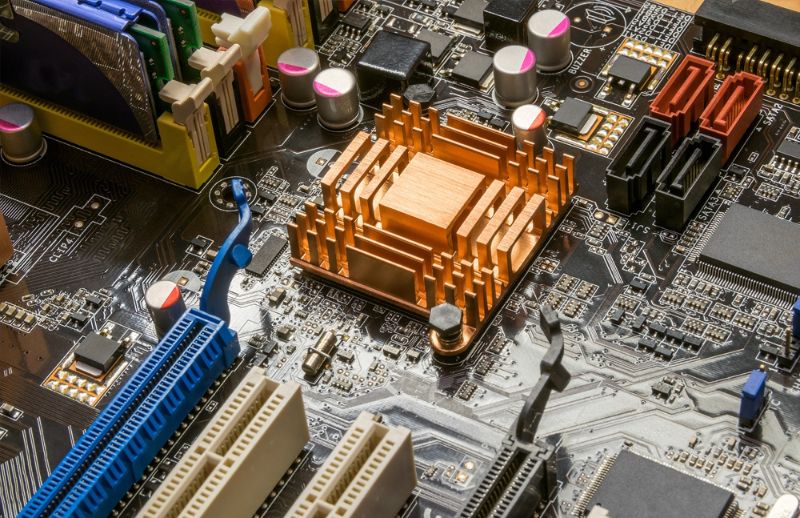
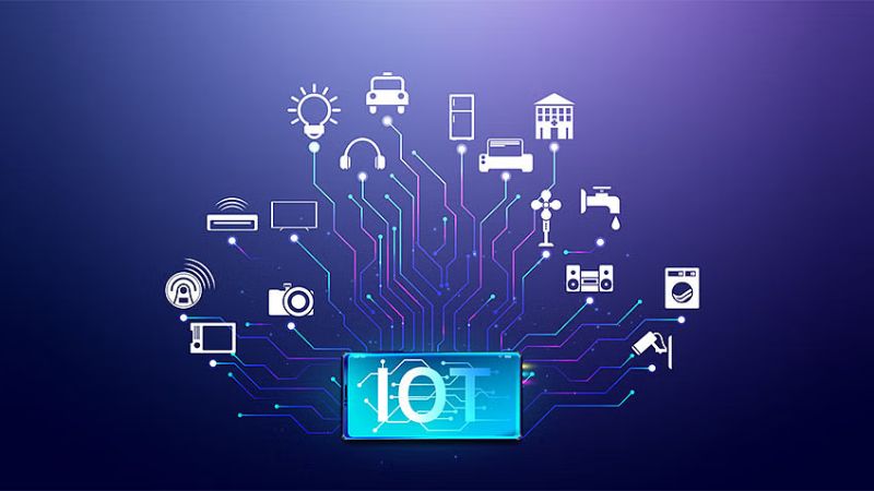
The landscape of technology is rapidly evolving, and at the forefront of this transformation is the Internet of Things (IoT). The IoT refers to the interconnected network of devices that communicate and exchange data seamlessly. IoT devices are becoming an integral part of our lives, from smart home appliances to industrial sensors. IoT PCB designs, particularly the circuit board design, plays a pivotal role in their functionality and efficiency. This article delves into the intricate challenges and innovative solutions involved in circuit board design for IoT devices.
Understanding IoT Device Requirements
IoT devices come in various shapes and sizes, united by common requirements. Compactness is essential, whether for wearable fitness trackers or industrial sensors. These devices must be lightweight and small enough to effortlessly fit into diverse environments. Moreover, optimizing power efficiency is paramount. Many IoT devices are battery-powered or rely on energy harvesting, necessitating meticulous power management to extend their operational lifespan. Striking the right balance between these factors demands a meticulous approach to designing a PCB.
Challenges in PCB Design for IoT Devices
Circuit board design faces numerous challenges due to the demand for smaller IoT devices. Designers are tasked with fitting an increasing number of components into a confined space, necessitating precise component placement, efficient trace routing, and overall layout optimization. These decisions significantly influence the device’s functionality, reliability, and pcb manufacture.
Miniaturization:
IoT devices are often characterized by their compact form factor, which presents a significant challenge in PCB design. As the demand for smaller and more discreet devices rises, PCB designers are tasked with squeezing an increasing number of components into a limited space. This miniaturization requires careful planning of component placement, routing of traces, and optimization of the overall layout. Each millimeter counts, and even seemingly minor decisions can have a substantial impact on the device’s functionality, reliability, and manufacturability.
Power Management:
IoT devices are frequently battery-powered or rely on energy harvesting techniques. Ensuring efficient power management is crucial to extend battery life and enhance the device’s operational longevity. Designers need to employ techniques such as voltage regulation, power gating, and low-power components to minimize energy consumption during active and idle periods. Achieving the right balance between performance and power efficiency is a delicate task that demands a deep understanding of the device’s usage patterns and power requirements.
Signal Integrity:
Maintaining signal integrity becomes progressively challenging in compact IoT devices due to the close proximity of traces and components. High-speed signals, especially in devices with wireless connectivity, are susceptible to interference, noise, and crosstalk. Designers must employ techniques like controlled impedance routing, signal shielding, and minimizing signal trace lengths to mitigate these effects and ensure reliable communication between components.
Wireless Connectivity:
The wireless connectivity of IoT devices is a double-edged sword. While it enables seamless communication and data exchange, it introduces challenges related to integrating wireless modules and antennas. Ensuring proper antenna placement, RF signal isolation, and efficient transmission and reception of signals is essential for reliable connectivity. The proximity of other components can impact antenna performance, making antenna design and placement a critical consideration.
Thermal Management:
The high component density in IoT devices, coupled with their small size, often leads to heat accumulation and inadequate heat dissipation. Overheating can degrade component performance, reduce lifespan, and even trigger premature failures. Effective thermal management strategies, such as optimizing component placement, employing heat sinks, and designing for efficient airflow, are necessary to prevent heat-related issues and maintain device reliability.
Component Integration:
IoT devices often encompass a diverse range of components, including sensors, microcontrollers, memory modules, and wireless chips. Integrating these components within a limited space requires meticulous planning to avoid conflicts, optimize signal paths, and maintain the device’s intended functionality. Complex routing, layer stacking, and utilizing multi-functional components are strategies employed to maximize integration without sacrificing performance.
Environmental Factors:
IoT devices are designed to function in various environments, from controlled indoor settings to outdoor and industrial environments. Designing PCBs that can withstand temperature fluctuations, humidity, dust, and other environmental challenges is essential to ensure consistent and reliable operation. Selecting appropriate materials, conformal coatings, and protective enclosures are strategies employed to enhance environmental resilience.
Cost Constraints:
While meeting design specifications is important, keeping production costs within budget is equally vital. IoT devices are often mass-produced, necessitating cost-effective design choices without compromising quality. Balancing the use of cost-efficient components, optimizing manufacturing processes, and reducing complexity are strategies to ensure that the final product remains competitive in the market.
Security Considerations:
IoT devices are often part of interconnected networks, making them susceptible to cybersecurity threats. Designing PCBs with built-in security features, such as hardware encryption, secure boot, and tamper detection, requires a deep understanding of cybersecurity principles. Ensuring that data remains confidential and the device is resistant to unauthorized access adds an additional layer of complexity to the design process.
Interference and Noise:
The compact nature of IoT devices makes them susceptible to electromagnetic interference (EMI) and radio frequency interference (RFI). These unwanted electromagnetic disturbances can disrupt signals, degrade performance, and lead to data corruption. Employing proper grounding techniques, signal shielding, and layout optimization are essential to mitigate the effects of interference and noise.
Regulatory Compliance:
Depending on the application and region of deployment, IoT devices must adhere to specific regulatory standards and certifications. Designing PCBs that meet these standards while maintaining optimal functionality requires careful consideration of electromagnetic compatibility (EMC), radio frequency (RF) emissions, and safety requirements. Non-compliance can lead to delays in product launch and market entry.
Heterogeneous Integration:
Many IoT devices combine various technologies on a single board, such as microcontrollers, sensors, communication modules, and power management circuits. Integrating these diverse technologies while ensuring that they operate harmoniously is a multifaceted challenge. Designers must manage thermal compatibility, signal isolation, and potential conflicts between functional blocks.
Solutions and Strategies
Addressing the myriad challenges in PCB design for IoT devices requires a combination of innovative solutions and strategic approaches. Here, we’ll explore some key strategies that designers can employ to overcome these challenges and create IoT devices that excel in performance, reliability, and functionality.
Advanced PCB Design Tools:
Modern PCB design software plays a pivotal role in addressing the unique challenges posed by IoT devices. Advanced tools offer features like auto-routing, impedance control, and thermal analysis that aid in optimizing layouts for signal integrity and thermal performance. Simulation capabilities allow designers to predict and mitigate potential issues, minimizing the need for costly design iterations.
Multi-Layer Design:
Leveraging multiple PCB layers is a powerful technique to accommodate the growing number of components in IoT devices. Multi-layer designs allow for denser layouts without compromising on signal integrity. Designers can allocate specific layers for power and ground planes, reducing noise and improving electromagnetic compatibility.
Component Selection:
Selecting components that align with the specific requirements of IoT devices is paramount. Low-power microcontrollers, energy-efficient sensors, and wireless modules with optimal transmission ranges are crucial choices. Collaborating closely with component manufacturers helps designers understand the trade-offs between power consumption, performance, and cost.
Power-Efficient Designs:
To address power management challenges, designers can implement techniques such as power gating and sleep modes. These methods allow components to enter low-power states when not in use, significantly extending battery life. Moreover, employing efficient voltage regulators ensures that power delivery is optimized for each component’s needs.
RF Design Considerations:
For IoT devices with wireless connectivity, RF design is a critical aspect. Proper layout and placement of antennas are essential to achieve reliable wireless communication. By minimizing interference, optimizing impedance matching, and adhering to RF design best practices, designers can enhance the overall performance of wireless components.
Thermal Design Techniques:
Incorporating effective thermal management techniques is vital to prevent heat-related issues. Heat sinks, thermal vias, and layout optimizations that facilitate airflow are valuable strategies. Employing materials with high thermal conductivity and distributing heat-generating components evenly contribute to efficient heat dissipation.
Design for Manufacturing (DFM):
Designing with manufacturability in mind streamlines the transition from design to production. Collaborating with manufacturers during the design phase ensures that the chosen components, materials, and design features are compatible with manufacturing processes. This approach minimizes unexpected challenges during production.
Prototyping and Testing:
Prototyping and testing are indispensable phases in IoT PCB design. Iterative prototyping allows designers to validate their design choices and identify potential issues early. Rigorous testing under real-world conditions helps refine the design and ensures that the final IoT device meets performance and reliability expectations.
Role of PCB Assembly and Manufacture
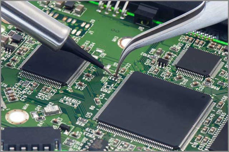
The design journey doesn’t end with the completion of the PCB layout. PCB assembly, the process of soldering components onto the board, is a crucial step that demands precision and attention to detail.
PCB Assembly Process:
The assembly process involves several stages, including component placement, solder paste application, soldering through reflow ovens or wave soldering machines, and quality inspections. Automated assembly machines ensure accurate component placement and consistent soldering quality.
Quality Control:
Quality control measures, such as visual inspections, automated optical inspections (AOI), and X-ray scans, are critical to ensuring that each solder joint is properly formed and that no defects are present. Robust quality control guarantees the reliability and functionality of the final IoT device.
Prototyping vs. Mass Production:
The assembly process can differ between prototypes and mass production. Prototyping often involves manual assembly to quickly validate the design. In contrast, mass production utilizes automated assembly lines to ensure efficiency and consistency at scale.
Case Studies
Real-world case studies provide valuable insights into how challenges in PCB design for IoT devices can be effectively addressed. Let’s delve into a couple of illustrative examples:
Case Study 1: Wearable Health Monitor
Challenge: Designing a wearable health monitor that tracks vital signs and wirelessly transmits data in real-time while maintaining a small form factor.
Solution:
- Component Selection: Careful selection of low-power sensors and microcontrollers optimized for wearable applications.
- Multi-Layer Design: Utilizing multiple PCB layers to accommodate components while ensuring a compact size.
- RF Design: Designing a compact yet efficient antenna layout to ensure reliable wireless communication.
- Power Management: Implementing power-saving modes to extend battery life without sacrificing functionality.
- Thermal Management: Integrating thermal vias and heat sinks to dissipate heat generated by sensors and wireless modules.
Case Study 2: Industrial IoT Gateway
Challenge: Creating an industrial IoT gateway capable of connecting numerous sensors and devices in a harsh environment while maintaining reliability.
Solution:
- Environmental Factors: Designing the PCB with rugged materials and conformal coatings to withstand extreme temperatures and humidity.
- Wireless Connectivity: Incorporating high-performance wireless modules with industrial-grade connectivity protocols.
- Component Integration: Carefully arranging components to minimize electromagnetic interference and ensure signal integrity.
- Thermal Design: Employing advanced thermal simulation tools to optimize heat dissipation in demanding conditions.
- Security Considerations: Integrating hardware security modules and encryption protocols to safeguard data transmissions.
Future Trends in IoT PCB Design
The landscape of IoT is continuously evolving, and as it does, so does the realm of PCB design. Several trends are shaping the future of IoT PCB design:
-
5G Integration:
The rollout of 5G networks will necessitate PCB designs capable of handling higher data rates and increased connectivity demands.
-
Edge Computing:
IoT devices are increasingly processing data at the edge, driving the need for efficient, power-conscious PCB designs that can handle local computation.
-
Flexible Electronics:
Flexible PCBs enable conformal designs that can adapt to irregular shapes, expanding the possibilities for IoT applications.
-
Energy Harvesting:
Advancements in energy harvesting technologies will require PCBs that can efficiently integrate and manage power from various sources.
-
AI and Machine Learning:
IoT devices are incorporating AI and machine learning capabilities, leading to PCB designs optimized for neural networks and efficient data processing.
Conclusion
IoT PCB design is a dynamic endeavor that demands a holistic understanding of challenges and a proactive approach to solutions. As the IoT landscape continues to expand, the role of skilled PCB designers becomes ever more crucial. By embracing innovative strategies, leveraging advanced tools, and adapting to emerging trends, designers can navigate the intricate terrain of IoT PCB design and contribute to the development of IoT devices that push the boundaries of innovation and functionality.