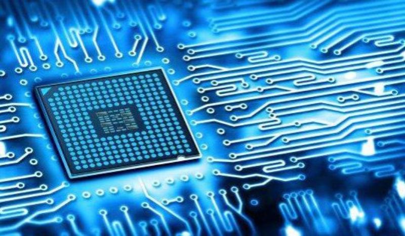
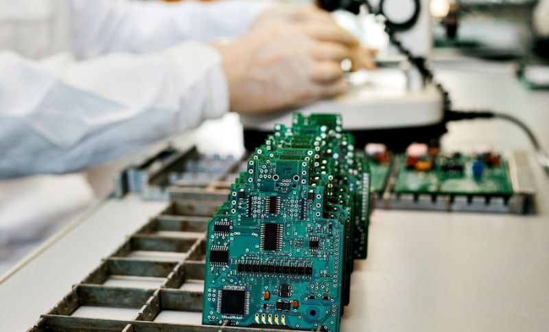
Printed Circuit Boards (PCBs) are the unsung heroes of modern electronics. These flat, often green boards are the backbone of nearly all electronic devices, from the smartphone in your pocket to the control panel of an industrial machine. PCBs have played an integral role in the miniaturization, efficiency, and functionality of electronic gadgets, and they continue to evolve alongside technological advancements.
This blog post will explore the latest trends and innovations in PCB fabrication techniques and materials. Keeping pace with these developments is crucial, as PCBs are at the heart of virtually every electronic system. Whether you’re an electronics enthusiast, a professional engineer, or someone merely curious about the inner workings of technology, this post will provide valuable insights into the state of PCB manufacturing today.
Significance of Staying Updated with PCB Fabrication Trends
Why should we care about the latest trends in PCB fabrication? The answer lies in the ever-increasing demands placed on electronic devices. Consumers expect smaller, more powerful, and energy-efficient gadgets. Industries require reliable electronics for automation, data processing, and communication. To meet these expectations, PCBs must continuously evolve.
Staying updated with PCB fabrication trends offers several advantages:
- Enhanced Performance: New fabrication techniques and materials enable the creation of PCBs that can handle high-speed signals, reduce energy consumption, and operate under extreme conditions.
- Miniaturization: Smaller, denser PCBs are essential for the development of compact electronic devices, wearable technology, and IoT applications.
- Reliability: Innovations in PCB fabrication lead to increased durability and resistance to environmental factors, critical for applications in harsh conditions.
- Sustainability: As environmental concerns grow, eco-friendly materials and sustainable manufacturing practices in PCB fabrication become a priority.
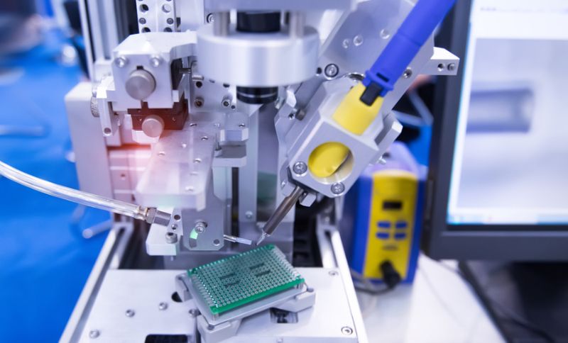
PCB Fabrication Techniques
PCB fabrication techniques encompass the processes and methods used to create printed circuit boards, which are essential components of electronic devices. This section’ll dive deeper into these techniques to understand their intricacies and applications.
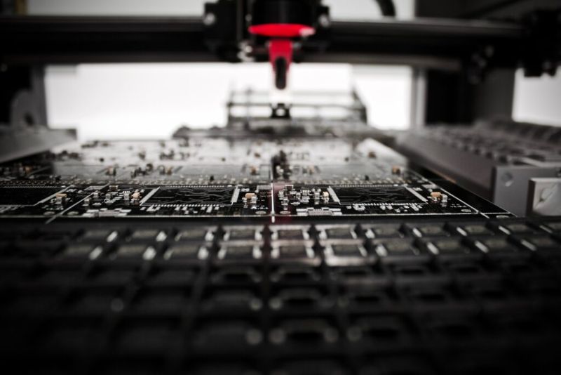
Traditional PCB Fabrication Process
The traditional PCB fabrication process involves several key steps, including substrate material selection, layer stacking, copper foil etching, drilling, solder mask application, and component assembly.
Traditional PCB fabrication is still widely used in various applications, particularly when cost-effectiveness and simplicity are priorities. It is suitable for standard consumer electronics, industrial controls, and automotive applications.
High-Density Interconnect (HDI) Technology
HDI technology is a significant advancement in PCB fabrication that allows for the creation of PCBs with multiple layers and extremely fine circuitry. It involves microvias, blind vias, and buried vias, enabling a high component density on a small board.
HDI technology is ideal for applications where size constraints are critical, such as smartphones, tablets, and wearable devices. It also finds use in high-performance computing and aerospace electronics.
Additive Manufacturing (3D Printing) in PCB Fabrication
Additive manufacturing, including 3D printing, has found its way into PCB fabrication. This technique involves depositing material layer by layer to build PCBs, allowing for rapid prototyping and complex circuitry.
3D printing in PCB fabrication accelerates product development and is particularly valuable for rapid prototyping, research and development, and low-volume production runs.
Laser Direct Imaging (LDI) for Precision Circuit Patterns
Laser Direct Imaging (LDI) has replaced traditional photolithography for creating precise circuit patterns on PCBs. It utilizes lasers to directly expose photoresist material, enhancing accuracy and minimizing defects.
LDI technology is crucial in applications where precise circuit patterns are required, such as high-frequency RF (Radio Frequency) electronics, medical devices, and aerospace systems.
PCB Layout
PCB layout plays a pivotal role in the fabrication process. The latest trends in PCB layout design are geared toward optimizing the performance and functionality of electronic devices:
Miniaturization
As consumer electronics continue to shrink in size, PCB layouts must follow suit. Engineers are constantly finding innovative ways to reduce component footprints while maintaining functionality.
High-Speed Signal Routing
With the rise of high-frequency applications, routing signals with minimal interference has become a priority. Advanced routing techniques and materials ensure signal integrity.
Automated Layout Tools
PCB design software has evolved, incorporating AI and automation to assist engineers in creating efficient layouts. These tools streamline the design process and reduce errors.
PCB Materials
PCB materials are the substrates on which the electronic components are mounted, and they play a critical role in determining the performance and reliability of printed circuit boards. This section will delve deeper into PCB materials, discussing different types, their properties, and their applications.
The Significance of PCB Materials
Overview: PCB materials are the foundation of electronic circuits, serving as the component placement and interconnection platform. The choice of materials greatly influences factors such as electrical performance, thermal management, and reliability.
FR-4 and Standard PCB Materials
FR-4 (Fire-Resistant 4) is the most common standard PCB material. It is a glass-reinforced epoxy laminate known for its durability and cost-effectiveness.
Properties:
- Excellent electrical insulation
- Good mechanical strength
- Adequate thermal stability
- Wide availability and affordability
FR-4 is suitable for a wide range of applications, including consumer electronics, industrial controls, and automotive electronics.
High-Frequency PCB Materials
High-frequency PCB materials are designed to operate at radio frequency (RF) and microwave frequencies. They offer low dielectric loss and high signal integrity.
Properties:
- Low dielectric constant (Dk)
- Low dissipation factor (Df)
- Excellent signal transmission at high frequencies
High-frequency PCB materials are crucial in RF and microwave applications, including wireless communication devices, radar systems, and satellite communications.
Flexible PCB Materials
Flexible PCB materials, often referred to as flex circuits, are designed to be bendable or flexible. They enable the creation of curved or irregularly shaped PCBs.
Properties:
- Bendability and flexibility
- Lightweight
- Resistance to vibration and shock
Flexible PCB materials are used in applications where bending or flexibility is required, such as wearable electronics, medical devices, and aerospace systems.
Environmentally Friendly PCB Materials
Environmental concerns have led to the development of eco-friendly PCB materials that reduce the environmental footprint of electronics production.
Properties:
- RoHS-compliant (Restriction of Hazardous Substances)
- Lead-free
- Recyclable materials
Environmentally friendly PCB materials are used in electronics products that adhere to strict environmental regulations and sustainability standards.
Thermal Management Materials
Thermal management is crucial in PCB design to dissipate heat generated by electronic components. Specialized thermal materials are used for this purpose.
Properties:
- High thermal conductivity
- Low thermal resistance
- Insulation properties
Thermal management materials are essential in power electronics, LED lighting, and any application where heat dissipation is a concern.
Choosing the Right PCB Material
Selecting the appropriate PCB material depends on factors such as the intended application, operating environment, thermal requirements, and budget. Engineers and designers should consider these factors carefully to choose the right material that aligns with the project’s goals.
Electronics PCB
The integration of PCBs in modern electronic devices has transformed the way we live and work:
IoT Devices
IoT devices rely on compact and efficient PCBs to connect the physical and digital worlds. These devices are revolutionizing industries such as healthcare, agriculture, and smart homes.
Enhanced Gadgets
PCB advancements have created more powerful and feature-rich smartphones, tablets, and other consumer gadgets.
Automotive Electronics and Electric Vehicles
The automotive industry is increasingly dependent on advanced PCBs to drive innovations in electric vehicles, autonomous driving, and in-car entertainment systems.
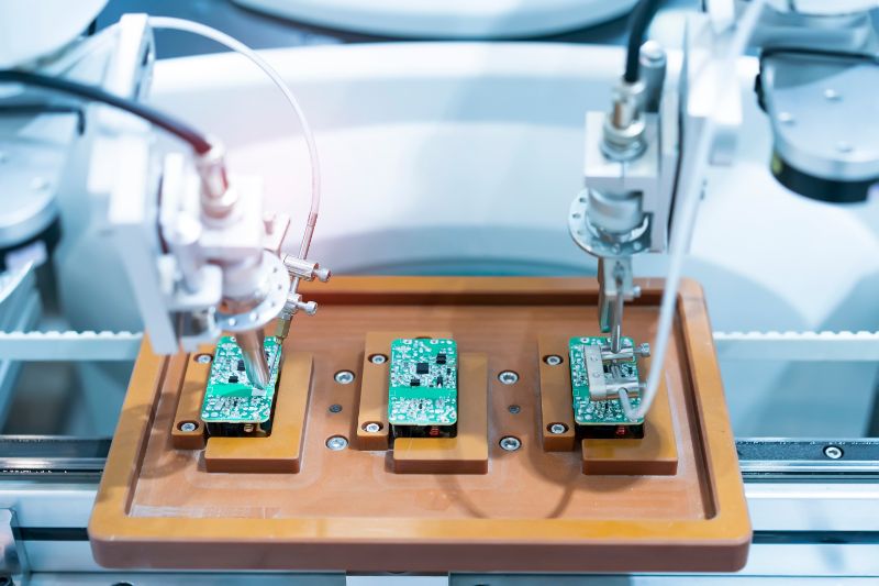
The Role of Contract Manufacturers
Contract manufacturers play a pivotal role in the PCB fabrication process. These specialized companies are experts in producing PCBs according to the specifications provided by their clients. In this section, we’ll explore the key aspects of contract manufacturers in the context of PCB fabrication.
The Role of Contract Manufacturers in PCB Fabrication
Contract manufacturers serve as external partners who handle various stages of PCB fabrication on behalf of their clients. They offer a range of services, including design assistance, prototype development, mass production, and quality control.
Expertise in the Latest PCB Fabrication Techniques
One of the primary advantages of working with contract manufacturers is their expertise in the latest PCB fabrication techniques and materials. These companies invest in staying up-to-date with industry advancements and employ skilled professionals who are well-versed in cutting-edge technologies.
State-of-the-Art Facilities
Contract manufacturers typically have state-of-the-art facilities with advanced machinery and equipment for PCB fabrication. This includes precision CNC machines, pick-and-place robots, and automated inspection systems. These facilities are optimized for efficiency and quality.
Quality Control and Assurance
Ensuring the quality and reliability of PCBs is of utmost importance. Contract manufacturers implement stringent quality control measures throughout the fabrication process. This includes inspections, testing, and adherence to industry standards and certifications.
Cost Efficiency
Working with contract manufacturers can often be more cost-effective than setting up an in-house PCB fabrication facility. By leveraging economies of scale and specialized expertise, contract manufacturers can offer competitive pricing for both prototype and large-scale production runs.
Design for Manufacturability (DFM) Support
Many contract manufacturers provide Design for Manufacturability (DFM) support, helping clients optimize their PCB designs for efficient and cost-effective production. This can include recommendations for component selection, layout adjustments, and design refinements.
Customization and Flexibility
Contract manufacturers offer a high degree of customization and flexibility. They can accommodate various PCB sizes, shapes, and specifications to meet different projects and industries’ unique needs.
Timely Delivery and Scalability
Meeting project deadlines is crucial in the electronics industry. Contract manufacturers are equipped to handle quick turnarounds and can scale production up or down as needed to accommodate changing demand.
Communication and Collaboration
Effective communication and collaboration between clients and contract manufacturers are essential for successful PCB fabrication projects. This includes regular updates, feedback loops, and transparency regarding project status and potential challenges.
Choosing the Right Contract Manufacturer
Selecting the right contract manufacturer is a critical decision. Clients should consider factors such as the manufacturer’s track record, industry experience, technical capabilities, and the alignment of their services with the project’s requirements.
Emerging Technologies and Future Trends
As the electronics industry continues its relentless march forward, several emerging technologies and future trends are poised to redefine the landscape of PCB fabrication. These innovations promise to revolutionize how we design and manufacture printed circuit boards, opening up exciting possibilities for smaller, more powerful, and environmentally friendly electronics.
Nanotechnology in PCB Fabrication
Nanotechnology, operating at the nanoscale, is becoming a game-changer in PCB fabrication. Nanomaterials, including nanocopper and nanosilver, offer impressive conductivity and thermal properties. This translates to PCBs that are not only smaller but also more efficient. Applications span a wide spectrum, from ultra-compact consumer devices to cutting-edge aerospace systems. However, working at such a minuscule scale presents unique challenges, demanding precision and specialized processes.
Quantum Computing and PCB Design
With its extraordinary computational power, Quantum computing brings forth a new set of challenges for PCB design. Quantum computers require specialized PCBs to support their complex architecture and the peculiar properties of quantum bits (qubits). The development of quantum-ready PCBs is already underway as pioneers in the industry explore innovative solutions to harness the full potential of this revolutionary technology.
Biodegradable PCBs
With growing environmental concerns, biodegradable PCBs are emerging as a sustainable alternative to traditional materials. The drive for more environmentally friendly electronics has led to the exploration of materials that break down naturally over time. These biodegradable PCB materials have the potential to reduce electronic waste and contribute to a greener electronics industry. Their applications range from eco-friendly consumer devices to environmentally conscious industrial solutions.
AI and Machine Learning in PCB Fabrication
Artificial intelligence (AI) and machine learning have become indispensable tools in optimizing PCB designs and ensuring quality control. AI can assist engineers in creating more efficient and cost-effective PCB layouts, streamlining the design process. On the other hand, machine learning is leveraged for predictive maintenance and quality control, helping manufacturers detect issues before they become critical, improving overall reliability.
Towards a Sustainable Future
The electronics industry is increasingly embracing sustainability, and a shift towards a circular economy is underway. Principles such as reducing, reusing, and recycling are being applied to electronics, including PCB fabrication. As we strive for a more sustainable future, it’s essential to recognize sustainable practices’ role in shaping the electronics industry. Sustainability isn’t just a buzzword; it’s a vital aspect of the path forward, ensuring that our innovations benefit both technology and the environment.
Conclusion
In the ever-changing landscape of electronics, staying informed about the latest PCB fabrication techniques and materials is not a luxury but a necessity. As this blog post has highlighted, advancements in PCB fabrication techniques, layout design, materials, and their applications are reshaping the electronics industry. Whether you’re an engineer, designer, or business owner, embracing these innovations can lead to more competitive, reliable, and sustainable electronic products. By understanding and leveraging the latest developments, you can position yourself and your projects at the forefront of the electronics industry.