RF PCBs are not often seen by the everyday designer, unless they are designing a board that includes WiFi/Bluetooth/LoRaWAN or other wireless communications capabilities. As these boards involve the use of analog signals and require precise oscillations in voltage and current to run properly, signal integrity is an extremely important aspect of RF PCB design.
With the rollout of 5G, broader use of IoT devices, applications like car/UAV radar, and other areas, many more designers will need to become familiar with some important points of RF PCB design. Engineering an RF PCB stack-up is vital to ensuring high frequency analog signals will not be corrupted due to crosstalk and EMI. If you’re planning to develop a new product with mixed signal or high frequency analog functions, I’ve compiled some important points on RF PCB stack-up design that can help you design successfully.
The Goals of RF PCB stack-up Design
Any stack-up should be designed to ensure signal and power integrity, but this is quite critical in RF design due to the requirements for clean analog signals (see the section on signal integrity below). The three most important points to consider in RF PCB stack-up design are:
- Isolation. The primary goal in RF PCB stack-up design is to ensure isolation between critical circuit blocks. As many RF systems are really mixed signal systems, isolation is critical for ensuring RF regions at different frequencies do not interfere with each other, and for ensuring analog signals do not interfere with digital signals. This is as much a layout problem as it is a stack-up design problem.
- Decoupling. This is something of a generic term. In terms of an RF PCB stack-up, this refers to sufficient decoupling between power and ground planes in order to ensure power integrity.
- Layer arrangement. At minimum, you should use a 4-layer PCB stack-up with internal power and ground planes. Power and ground planes can be placed in two adjacent internal layers, which provides decoupling and power integrity. Components can then be placed on a surface layer adjacent to the ground plane.
In addition to the three points mentioned above, you should consider your design decisions in the following two areas:
Decoupling and Power Integrity
I’ve discussed the importance of stack-up design in terms of power integrity in previous articles, but the same ideas apply to RF PCBs. The power integrity effects in an analog PCB are slightly different compared to a digital PCB, but the end goal of PDN design for an RF PCB is the same: ensure the power seen by your components does not fluctuate for any reason. This hinges on designing the right RF PCB stack-up and providing decoupling in your PDN.
Placing your stack-up and using properly-sized decoupling capacitors will ensure your board has the necessary level of decoupling to bring your PDN impedance down to a low value. In contrast to working with all-digital systems, you only need to worry about the target impedance at a narrow range of frequencies or at specific frequencies, rather than worrying about a broad bandwidth.

Decoupling capacitor self-resonance frequency examples. Your component manufacturer should be able to provide similar curves for your capacitors.
Any capacitors you use should have sufficiently high self-resonance frequency; some example capacitor insertion loss curves are shown above, and the self-resonance frequency is clearly visible. Decoupling will help ensure the PDN impedance is low enough to prevent PDN ripple. When you suppress ripple in your PDN, you then prevent jitter from propagating to the output of any RF oscillator you use for frequency synthesis
Your RF PCB stack-up and Signal Integrity
In terms of signal integrity, analog components are highly susceptible to noise. It is not that these components necessarily generate more noise than digital components. Instead, noise that is induced in an analog interconnect, whether it is from external radiated EMI or conducted EMI from another area of your board, will propagate into the input of a purely analog receiver component. This noise will then be passed through to the output of the component and will affect the operation of all downstream signals.
Why are analog components and signals so sensitive to noise? The reason is that analog components are generally run in the linear regime, whereas digital components are run at saturation. In digital components, the voltage simply needs to be above or below a certain threshold in order to be registered as a valid logic level. Any small variation in the signal level within a digital component’s noise margin will have no effect. This means noise on a digital signal has to be much larger to cause errors compared to an analog signal. With an analog signal, any noise seen at the input of an analog component generally produces some proportional change in the output signal level. This is why noise in analog circuits is so critical.
Johnson noise, pink noise, and shot noise are much less important in an RF PCB than crosstalk. A digital signal at only a few volts can induce strong capacities and inductive crosstalk in an analog signal during switching, but the reverse is not always the case. Analog signals generally need to be at a much higher signal level in order to generate crosstalk in a low-level digital signal. If you design your stack-up and layout correctly, you can isolate mixed signal boards and ensure high frequency analog signals, low frequency analog signals, and digital signals do not interfere with each other. This should underscore the importance of isolation in these systems.

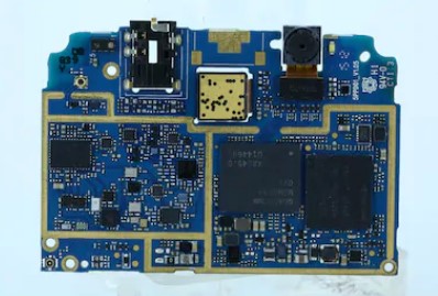
An example RF PCB with strong isolation.
Your stack-up and Layout
With your stack-up being so critical to passing EMI checks and ensuring RF signal integrity, you should start by considering the number of layers you need, and then determine how to arrange them so that you prevent EMI problems while ensuring a target impedance is met with your chosen routing style. Low layer count boards are most likely going to be unacceptable in an RF PCB. At minimum, you will need to use a higher layer count board in order to provide sufficient room for power, ground, and signal layers.
The typical set of materials used in an RF PCB stack-up will be low-loss laminates when operating above 5 GHz WiFi/Bluetooth frequencies. Standard or low-loss FR4 laminates will operate well at lower frequencies, including if routing RF signals through a wave-guide that confines the field to the inner layers of the PCB. The table shown below provides an overview of some Isola and Rogers materials that could be used in RF PCBs.

Some materials used in RF PCB stack-ups.
If PTFE laminates are used in the stack-up, a bondply will be used to provide the same function as prepreg in a standard FR4 stack-up. Other FR4 materials can still be used in the same way as in any other stack-up.
2-layer and 4-layer stack-ups
With 2-layer boards, you simply won’t have enough space to place printed circuits and impedance controlled traces unless everything is routed as coplanar lines. If for whatever reason, coplanar routing can’t be used in a 2-layer or 4-layer board, you will be forced to put ground on the back layer and wide traces will be needed for RF routing. For example, with a 1 mm thick substrate, the required trace width for microstrips without coplanar routing will be 80 mils; this is simply too wide.
4-layer stack-ups are technically a better entry-level option, including for mixed-signal boards. These stack-ups will require you place and route all RF signals and components on a single layer. Power, digital, and other peripherals can then be placed on the bottom layer, or you could use lower-frequency printed RF circuits on the bottom layer. If you need two signal layers, you can place GND on the two internal layers to provide isolation and impedance control on both layers.
6 or More Layers
A basic 6-layer stack-up is shown in the image below. Note that the dielectric layer supporting RF routing can be a low-loss PTFE laminate. This stack-up provides controlled impedance routing on the outer surface layers, and the plane layers will provide shielding between signal layers. In addition, the power and ground planes are placed adjacent on the same side of the core. This will provide greater decoupling than in a 4-layer PCB thanks to the higher interplane capacitance. The ground planes should also be linked with stitching vias to provide a consistent reference potential throughout the board.

Basic 6-layer RF PCB stack-up in Altium Designer.
This should be the starting point for thinking about an RF PCB stack-up. Folks like Rick Hartley recommend going for at least an 8-layer stack-up, and I tend to agree when more signals need to be routed. You can also check out the 10-layer stack-up I’ve created in this article for more guidance.
The idea behind this PCB stack-up is to enable a mixed-signal design approach with digital on two signal layers and RF on another signal layer. Placing an RF signal on the top layer enables 50 Ohm impedance routing with small trace widths and total isolation from the digital sections. The bottom layer can also be used for controlled impedance differential pairs for digital interfaces. Finally, the power/ground plane pair provides the required decoupling for power integrity to support any high speed digital interfaces.
Routing and Shielding
For signal traces on the surface layer, one common practice is to use ground copper pour and via fences shield different sections of the board. The grounded copper pour and vias provide image charge that strongly opposes any EMI radiated from a nearby board section. The via fences need to be precisely designed, although a good approximation for the case where the pour region is much larger than the diameter and spacing between vias is to set the spacing smaller than half the signal wavelength (in the dielectric) to prevent lowest order resonances between the vias. There are several basic simulation tools and calculators online that can be used for via fence/via gridding design on the surface layer.
Using coplanar wave-guides or substrate integrated wave-guides is a great routing strategy as these routing topologies provide excellent isolation. While these structures can be rather large compared to microstrip traces, these structures provide high levels of isolation and are already used in many microwave/mmWave devices.

This gridded PCB layout has exposed copper with stitching vias to separate different functional blocks into different regions of the board. The stitched vias provide some shielding so that functional blocks can be separated. The other reason for the exposed plated copper is to provide a direct conductive connection to the enclosure, which will also provide some shielding.