The PCB industry has made considerable strides in only a few decades. Today, multilayer printed circuit boards are increasingly popular due to their manifold benefits–ranging from higher density and enhanced functionality–in addition to potential drawbacks like greater susceptibility to environmental conditions such as electromagnetic radiation and moisture infiltration. With this in mind, let’s investigate the pros and cons of these advanced technologies so that you can make an informed decision when it comes any future printed circuit board purchases! Furthermore, we will provide guidance on how one may discern if their domicile is affected by multilayer PCBs presence for remediation steps should they be present at home.
What are Multilayer PCBs?

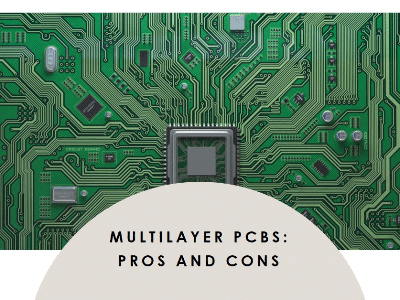
Multilayer PCBs, or multilayer printed circuit boards, are essentially a sandwich of multiple layers of conductive pathways separated by insulating materials. Unlike single-layer PCBs, which have only one layer of conductive material between the components and the wiring on the board, multilayer PCBs can have anywhere from two to dozens of layers.
Each layer is connected using vias – small holes drilled through all layers that allow electrical signals to pass through. Multilayer PCBs are typically used in applications where high-density circuits are required and space is limited.
The construction process for multilayer PCBs involves laminating together pre-drilled core sheets with copper foil and bonding them under heat and pressure. A final etching process removes excess copper from each layer, leaving behind only the desired traces.
With their ability to pack more functionality into less space and provide better signal integrity due to shorter interconnect paths between components, it’s no wonder why multilayer PCBs have gained popularity in recent years. However, as we’ll explore later in this post, there are also drawbacks associated with their use.
The Benefits of Multilayer PCBs
Multilayer PCBs offer several benefits over their single-layer counterparts. Firstly, they allow for more complex circuit designs as multiple layers can be used to connect components and reduce the overall size of the board. This allows for smaller devices that are more convenient and portable.
Secondly, multilayer PCBs offer improved signal integrity as they have a reduced risk of electromagnetic interference (EMI) due to the increased isolation between traces. They also have shorter trace lengths which result in lower resistance, capacitance and inductance which leads to faster signal transmission speeds.
Thirdly, multilayer PCBs provide better power distribution as they can incorporate multiple power planes which distribute power more evenly across the board while reducing voltage drops. This results in less noise on signals and a higher level of stability.
Multilayer PCBs are highly reliable due to their design redundancy where if one layer fails or has an issue it does not affect other layers. These benefits make multilayer PCBs essential for modern electronic technology that requires dense circuits with high-speed data transfer rates and efficient power management systems.
The Drawbacks of Multilayer PCBs
Despite the numerous benefits of multilayer PCBs, there are also some drawbacks to consider. One significant disadvantage is their complexity and cost. Multilayer PCBs require more materials, time and expertise to manufacture, which makes them more expensive than single or double-layered boards.
Another drawback is that they can be difficult to repair if something goes wrong. Unlike traditional PCBs where issues can often be easily identified and fixed, multilayer boards have many layers of components sandwiched together making it challenging to locate a problem area.
Furthermore, designing a multilayer PCB requires advanced knowledge in electronics and engineering software. This means that not every engineer has the necessary skills to design such complex circuitry.
Multilayer PCBs may also pose environmental concerns during disposal due to their multiple layers containing different types of electronic waste. If not disposed of properly, these types of printed circuit boards could contribute further pollution into our environment.
While there are several advantages for choosing multilayer PCBs over other types of circuits board options available in today’s market; it should be understood that they come with additional costs and complex manufacturing requirements. Moreover, careful consideration must be taken when disposing these printed circuit boards responsibly following proper regulations outlined for e-waste management practices
How to Tell if Your Home is Affected by Multilayer PCBs
Multilayer PCBs have been used in various applications for years, including electronic devices and building materials. However, if your home was built before the 1980s, it may contain materials that were manufactured using PCBs. Here’s how to tell if your home is affected by multilayer PCBs.
Firstly, you should look out for any signs of deterioration or damage to the building material. If there are cracks or holes in the walls or ceilings, this could be a sign that the material contains multilayer PCBs.
Another way to determine whether your home contains multilayer PCBs is through air testing. A professional can take samples of the air inside your home and test them for contaminants such as PCB particles.
It is vital to recognize that a multitude of commonplace items may contain traces of multilayer PCBs, such as old fluorescent light ballasts and certain sorts of caulk.
If you suspect that your abode may be harbouring multilayer PCBs, it’s critical to call in a skilled professional who can perform further investigations and offer guidance on what course of action should be taken. Failure to deal with potentially contaminating materials appropriately could later lead to both health issues for the house occupants and detrimental impacts on their lives in general.
Assessing the presence of multiple layers of PCBs requires careful observation and analysis from specialists; it’s always beneficial to err on the side of caution when it comes to potentially hazardous building materials, such as these!
What to Do If You Find Multilayer PCBs in Your Home
If you discover multilayer PCBs in your home, it’s essential to take immediate action. These boards contain hazardous chemicals and can pose a significant risk to your health.
The first step is to identify the source of the PCBs. If you suspect that they are present in building materials such as insulation or caulking, contact a professional environmental testing service for an inspection.
If multilayer PCBs are found in your home, it’s important to seal off any contaminated areas immediately and restrict access until remediation is complete. Avoid touching or disturbing the contaminated material as this could release toxic particles into the air.
Seek professional help from qualified experts who specialize in removing hazardous materials safely. They have specialized equipment and training to remove and dispose of multilayer PCBs without causing further contamination.
After removal, make sure all surfaces are thoroughly cleaned with appropriate cleaning solutions specifically designed for this type of cleanup. Be proactive by educating yourself about potential sources of exposure and taking steps to prevent future contamination.
Finding multilayer PCBs in your home may seem overwhelming at first but taking swift actions will ensure you protect yourself from harmful effects while keeping others safe too.