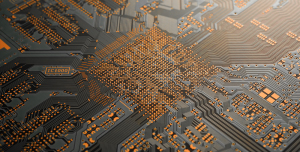
Designing high-speed PCBs is a complex and critical task in today’s electronics industry. As electronic devices become faster and more advanced, the demand for high-speed PCBs has increased significantly. These PCBs carry signals with fast edge rates, high-frequency clocks, and tight timing margins. Designing them requires meticulous attention to detail and adherence to best practices to ensure optimal performance and signal integrity.
This blog post will explore essential tips and techniques for designing high-speed PCBs. From understanding high-speed signals to managing electromagnetic interference (EMI), we will cover key aspects of high-speed PCB design. Whether you are a seasoned PCB designer or just starting, these insights will help you confidently tackle high-speed design challenges.
Understanding High-Speed PCBs
Before delving into the intricacies of high-speed PCB design, it’s essential to grasp the characteristics and challenges of high-speed signals. High-speed PCBs carry signals with frequencies typically in the range of hundreds of megahertz to several gigahertz. At these frequencies, the PCB layout, trace impedance, and signal integrity become critical factors affecting overall performance.
High-speed signals are susceptible to phenomena such as reflection, crosstalk, and attenuation. A thought occurs when a signal encounters an impedance mismatch, leading to signal degradation and potential data errors. Crosstalk happens when signals from one trace interfere with nearby traces, impacting signal integrity and causing cross-channel noise. Moreover, high-speed signals can experience attenuation, where signal strength diminishes over long trace lengths, necessitating careful signal management.
To address these challenges effectively, PCB designers must consider signal integrity principles, transmission line theory, and proper termination techniques during the design process.
Pre-Design Preparation
An essential step in high-speed PCB design is thorough pre-design preparation. This phase involves defining project requirements, identifying critical signal paths, and selecting appropriate materials.
Defining Project Requirements and Specifications
Defining project requirements and specifications entails understanding the desired performance parameters of the PCB. The required clock speeds, data rates, and signal tolerances are key factors. Additionally, considering the intended application and environmental conditions will help determine the PCB’s form factor and material requirements.
Selecting Appropriate Materials for High-Speed PCBs
Selecting appropriate materials for high-speed PCBs is crucial for achieving signal integrity and minimizing losses. High-quality materials with controlled dielectric constants and low dissipation factors are preferred for reducing signal reflections and maintaining signal integrity. The choice of materials is especially critical when designing a PCB for high-speed applications, as the dielectric properties directly impact signal propagation.
Identifying Critical Signal Paths
Identifying critical signal paths involves recognizing the traces that carry high-speed signals and are most susceptible to signal degradation. Focusing on these vital paths during design allows for targeted optimization and signal management. Properly designed signal paths ensure minimal signal distortion and reduced signal degradation, ensuring that high-speed signals reach their destination accurately and reliably.
High-Speed PCB Layout Techniques
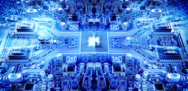
The PCB layout plays a pivotal role in high-speed design. An optimized layout minimizes signal distortion, reduces crosstalk, and ensures signal integrity. Here are some key layout techniques to consider:
Signal Layer Stackup and Impedance Control
High-speed PCBs often require controlled impedance traces to match the characteristic impedance of the transmission lines. Proper layer stack up with controlled dielectric thickness and trace width helps achieve consistent impedance across the PCB. The correct layer stack-up ensures that high-speed signals propagate efficiently, reducing signal reflections and signal integrity issues.
Proper Placement of High-Speed Components
Placing high-speed components strategically reduces trace lengths, minimizes signal delays, and optimizes signal paths. Components that require high-speed signal processing, such as microcontrollers, FPGAs, and high-speed memory, should be placed thoughtfully to enhance signal flow. The placement of high-speed components is essential in designing a PCB to ensure efficient signal propagation and minimal signal distortions.
Minimizing Parasitic Effects and Noise
Parasitic effects, such as capacitance and inductance, can degrade signal quality. Minimizing trace lengths, using ground stitching vias, and employing guard traces help mitigate parasitic effects. Eliminating or reducing parasitic effects is vital for minimizing signal degradation and ensuring accurate and reliable high-speed signal transmission.
Routing Strategies for High-Speed Traces
High-speed traces should follow best routing practices to reduce signal reflections and crosstalk. Techniques like length matching, differential pair routing, and controlled-impedance vias are essential for preserving signal integrity. Careful routing ensures that high-speed signals propagate without interference, preserving the quality and integrity of the transmitted data.
Differential Pairs and Their Design Considerations
Differential pairs are commonly used for high-speed data transmission. Keeping the two traces of a differential pair close together and maintaining equal lengths is vital for preserving the balance and integrity of the signal. Proper design considerations ensure the differential pairs function effectively, reducing noise and ensuring reliable high-speed data transmission.
The careful implementation of these layout techniques ensures high-speed signals can propagate efficiently and accurately throughout the PCB.
Power Integrity and Decoupling Techniques
Ensuring power integrity is critical in high-speed PCB design, as power distribution affects signal quality and overall performance. Rapid changes in current demand from high-speed components can lead to voltage fluctuations and noise, affecting signal stability. To address power integrity concerns:
Importance of Power Integrity in High-Speed PCBs
Power distribution networks must be designed to deliver stable and noise-free power to critical components. Any voltage fluctuations or noise on the power rails can cause signal jitter and data errors. Proper power integrity measures are essential in designing a PCB to ensure that the high-speed components receive the required power without signal degradation.
Decoupling Capacitor Selection and Placement
Proper decoupling capacitors provide localized energy storage to high-speed components, minimizing voltage fluctuations during transient current demands. Selecting appropriate capacitor values and placing them close to the power pins of components is vital for effective decoupling. Proper decoupling ensures that the high-speed components receive stable and clean power, enhancing overall signal integrity and performance.
Ground Plane Design and Its Impact on Power Integrity
A solid ground plane is essential for providing a low-impedance return path for high-speed signals and minimizing ground bounce. Ensuring a well-defined and continuous ground plane is crucial for managing power integrity. An optimized ground plane design is essential in PCB manufacturing, ensuring that the high-speed signals have a low-impedance return path, reducing noise and enhancing signal integrity.
Incorporating power integrity techniques in the PCB design ensures that high-speed components receive stable and clean power, enhancing overall signal integrity and performance.
Signal Integrity Analysis and Simulation
Before moving forward with the final layout, performing signal integrity analysis and simulation is essential to predict and mitigate potential issues. Signal integrity analysis tools assist in identifying signal reflections, crosstalk, and other signal integrity problems.
Introduction to Signal Integrity Analysis Tools
Signal integrity analysis tools like Hyperlynx, SIWave, and Altium Designer’s PDN Analyzer are commonly used in high-speed PCB design and PCB manufacturing. These tools provide a detailed understanding of signal behavior and help identify areas that require improvement. Using signal integrity analysis tools ensures that high-speed signals meet the required performance specifications.
Performing Pre-layout Signal Integrity Simulations
Pre-layout simulations enable designers to assess signal integrity before finalizing the PCB layout. These simulations predict potential signal integrity issues, guiding designers in making informed decisions during the layout phase. Some key pre-layout simulations include:
- Eye Diagram Analysis: Eye diagram simulations evaluate signal quality by plotting the superimposed waveforms of multiple data bits. A clean and open-eye diagram indicates good signal quality.
- Reflection Analysis: Pre-layout reflection analysis helps identify impedance mismatches and potential signal reflections that can lead to signal degradation.
Post-layout Signal Integrity Validation and Analysis
Post-layout simulations validate the signal integrity of the finalized PCB layout. They ensure that the implemented design meets the required performance specifications. Key post-layout simulations include:
- Time Domain Reflectometry (TDR): TDR measurements assess the impedance profile of traces and provide insight into signal reflections and impedance mismatches.
- S-Parameters Analysis: S-parameter simulations evaluate signal behavior between different ports and assess crosstalk and transmission line performance.
Identifying and Resolving Signal Integrity Issues
Analyzing simulation results helps identify signal integrity issues, such as signal reflections, crosstalk, and timing violations. Designers can then implement appropriate design changes to address these issues effectively. Identifying and resolving signal integrity issues are crucial in designing a PCB to ensure optimal signal performance and reliability.
By performing comprehensive signal integrity analysis and simulation, designers can ensure the reliability and robustness of high-speed PCB designs.
EMI/EMC Considerations in High-Speed Design
High-speed PCB designs often face Electromagnetic Interference (EMI) and Electromagnetic Compatibility (EMC) challenges. EMI refers to unwanted electromagnetic emissions that can interfere with other electronic components and systems. At the same time, EMC is the ability of a device to operate in its electromagnetic environment without causing interference. Ensuring EMI/EMC compliance is essential for properly functioning high-speed PCBs and successful PCB manufacturing. This section will explore the considerations and techniques to minimize EMI and achieve EMC compliance.
Understanding EMI/EMC Challenges in High-Speed PCBs
EMI can arise from various sources, including fast-switching edges, high-frequency clock signals, and signal traces acting as antennas. High-speed PCBs are particularly susceptible to EMI due to the increased frequency of their signals in PCB manufacturing. Common challenges include:
- Crosstalk: Crosstalk occurs when signals from one trace interfere with nearby traces, leading to signal distortion and potential errors. Proper signal isolation techniques are vital to minimize crosstalk.
- Radiated Emissions: High-speed signals can radiate electromagnetic energy, which can affect nearby components and devices. Managing radiated emissions is crucial to avoid interference with other electronic systems during PCB manufacturing.
Techniques to Reduce Electromagnetic Interference (EMI)
Reducing EMI involves adopting various design techniques to mitigate electromagnetic emissions and susceptibility in designing a PCB. Some effective techniques include:
- Signal Isolation: Keeping sensitive traces away from high-speed signal traces and power lines helps minimize EMI in PCB manufacturing. Properly separating critical signals from noisy ones reduces the chances of interference.
- Ground Plane Segmentation: Dividing the ground plane into smaller segments can help control the return paths for high-speed signals and reduce ground bounce, contributing to lower EMI during PCB manufacturing.
Shielding and Grounding Strategies for EMC Compliance
EMC compliance requires the PCB to be designed with appropriate shielding and grounding techniques during PCB manufacturing. These strategies help contain electromagnetic emissions and protect the PCB from external interference:
- Shielding: Adding conductive shielding, such as metal enclosures or copper shielding cans, around sensitive components can prevent EMI from escaping and shield the components from external interference during PCB manufacturing.
- Proper Grounding: Ensuring a solid and low-impedance ground connection is essential for controlling EMI during PCB manufacturing. Effective grounding techniques include star grounding and using ground planes to provide a low-resistance return path for high-speed signals.
Thermal Management for High-Speed PCBs
High-speed PCBs often generate significant heat due to the increased power consumption and current flow in high-speed components. Proper thermal management is crucial to maintain the performance and reliability of the PCB. In this section, we will explore various thermal management techniques for high-speed designs.
Thermal Challenges in High-Speed Designs
Thermal challenges in high-speed PCBs arise from the power dissipation of high-speed components and the compact layout of the board. Insufficient heat dissipation can lead to temperature rise and adversely affect component performance, causing signal integrity issues and potential failures during PCB manufacturing.
Thermal Relief Techniques for High-Power Components
To dissipate heat effectively, thermal relief techniques are employed, especially for high-power components such as microprocessors, FPGAs, and power amplifiers during PCB manufacturing. Some common thermal relief techniques include:
- Heat Sinks: Heat sinks are passive cooling devices that dissipate heat away from high-power components. They are attached to the component’s surface, increasing the surface area for better heat dissipation in PCB manufacturing.
- Thermal Vias: Thermal vias are copper-filled vias that conduct heat from the component’s thermal pad to the inner or outer layers of the PCB. They act as thermal pathways, allowing heat to move away from the component during PCB manufacturing.
Cooling Strategies to Prevent Overheating
In addition to thermal relief techniques, cooling strategies play a crucial role in high-speed PCBs’ thermal management during PCB manufacturing:
- Active Cooling: Active cooling methods, such as fans or liquid cooling, can be employed for high-power components that require additional heat dissipation beyond passive techniques during PCB manufacturing.
- Optimized PCB Layout: An optimized PCB layout that considers the placement of high-power components and heat-generating elements can improve heat dissipation and prevent hotspots on the board during PCB manufacturing.
Maintaining appropriate temperatures through efficient thermal management ensures the reliability and longevity of high-speed PCBs during PCB manufacturing.
Design for Manufacturability (DFM) and Design for Testability (DFT)
Design for Manufacturability (DFM) and Design for Testability (DFT) are critical aspects of high-speed PCB design during PCB manufacturing. Ensuring that the PCB design is manufacturable and testable simplifies the manufacturing and testing processes, reduces production costs, and enhances overall quality. In this section, we will explore the considerations for DFM and DFT in high-speed PCB designs.
DFM Considerations for High-Speed PCB Fabrication
DFM aims to optimize the PCB design for efficient and cost-effective manufacturing during PCB manufacturing. High-speed PCBs present specific challenges, and considering DFM principles during the design phase can streamline the fabrication process. Some important DFM considerations include:
- Minimum Trace Width and Spacing: High-speed PCBs may require smaller trace widths and spacing to maintain signal integrity during PCB manufacturing. However, these should still be manufacturable within the PCB manufacturer’s capabilities.
- Impedance Control and Tolerances: Ensuring that the controlled impedance traces are within the manufacturer’s fabrication tolerances is essential for consistent signal performance during PCB manufacturing.
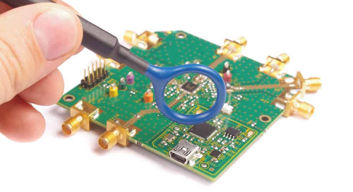
DFT Techniques to Facilitate Testing and Debugging
Design for Testability (DFT) focuses on incorporating features into the PCB design that facilitate testing and debugging during production and assembly during PCB manufacturing. Some common DFT techniques include:
- Test Points: Including test points on the PCB allows easy access for testing and debugging purposes, simplifying the troubleshooting process during PCB manufacturing.
- Boundary Scan (JTAG): Implementing boundary scan (Joint Test Action Group) technology allows for efficient testing of interconnected components and nets during PCB manufacturing.
Collaboration with Manufacturers for Seamless Production
Collaboration between PCB designers and manufacturers is essential for successful high-speed PCB production during PCB manufacturing. Working closely with manufacturers ensures that design requirements and specifications are met, potential manufacturing challenges are addressed, and any necessary design adjustments are made to improve manufacturability and testability during PCB manufacturing.
Future Trends in High-Speed PCB Design
The world of high-speed PCB design constantly evolves with materials, technologies, and applications advancements. As electronic devices continue to push the boundaries of speed and performance, PCB designers must stay ahead of the curve during PCB manufacturing. In this section, we will explore some future trends in high-speed PCB design.
Advancements in High-Speed Materials and Technologies
Researchers and manufacturers continuously develop high-speed materials with enhanced dielectric properties and reduced signal loss during PCB manufacturing. Advancements in material technologies, such as low-loss laminates and high-frequency substrates, enable the design of high-speed PCBs with improved performance during PCB manufacturing.
The Impact of Emerging Technologies on High-Speed PCBs
Emerging technologies like 5G, the Internet of Things (IoT), and autonomous vehicles demand increasingly sophisticated electronic systems. High-speed PCBs play a vital role in these technologies, and designers must adapt to the specific requirements and challenges presented by these applications.
Conclusion
This comprehensive blog post has explored a wide range of tips and techniques for designing high-speed PCBs. Each aspect is crucial for successful high-speed design, from understanding high-speed signals and layout techniques to managing thermal challenges and ensuring manufacturability and testability. Additionally, staying updated with future trends and emerging technologies will empower designers to meet the demands of tomorrow’s high-speed electronic systems.
As the electronics industry continues to evolve, high-speed PCB design will remain at the forefront of innovation. By applying the knowledge and best practices covered in this blog post, designers can navigate the complexities of high-speed PCB design and create cutting-edge electronic devices that shape the future of technology.