The PCB market is booming and is expected to reach a staggering $93.87 billion by 2029. However, as electronics shrink and functionalities explode, traditional PCB manufacturing methods are reaching their limits.
To keep pace, the industry must implement groundbreaking advancements in processes and materials. This guide is compiled to help you learn about these trends.
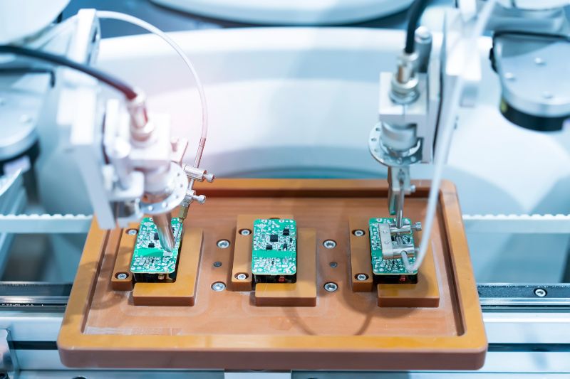
This blog will introduce you to the exciting trends that the best manufacturers use nowadays. You will see how PCBLOOP’s manufacturers use cutting-edge technologies like artificial intelligence and 3D printing to shape the future of PCBs, paving the way for a future of high-performance, miniaturized electronics.
Without any further ado, let’s take a look at them!
The Advanced Processes
First, let us introduce you to some trending advanced processes:
Artificial Intelligence (AI) and Machine Learning (ML)
Artificial Intelligence (AI) and Machine Learning (ML) are shifting the paradigm from reactive troubleshooting to proactive prediction, optimizing every stage of the PCB layout and production process.
Here’s how AI and ML are revolutionizing PCB manufacturing:
- Predictive Maintenance: Traditional methods rely on reactive maintenance, fixing equipment breakdowns after they occur. AI and ML analyze vast datasets of sensor data, identifying patterns and predicting potential equipment failures before they happen. This allows for preventative maintenance, reducing downtime, and ensuring a smooth production flow.
- Optimized PCB Layout Design: AI algorithms can analyze complex design rules and constraints to create highly optimized PCB layouts. These layouts consider factors like signal integrity, thermal management, and manufacturability, leading to improved performance and manufacturability. Companies offering PCB layout services can leverage AI to provide faster turnaround times and more efficient designs.
- Real-Time Quality Control: ML algorithms can be trained on historical data to identify potential quality issues during PCB manufacturing. By analyzing real-time data from inspection systems, AI can flag potential defects before they become embedded in the final product. This proactive approach reduces the number of faulty boards and ensures consistent quality for companies offering PCB layout design services.
Benefits of AI and ML in PCB Manufacturing
- Increased Productivity: Predictive maintenance and optimized layouts lead to fewer production delays and rework, ultimately boosting overall productivity.
- Reduced Downtime: AI minimizes unexpected downtime by proactively addressing potential equipment failures keeping production lines running smoothly.
- Lower Costs: Reduced rework, fewer defects, and optimized processes translate to significant cost savings for PCB manufacturing service providers.
Additive Manufacturing Techniques
On Number two, it is Additive Manufacturing (AM), also known as 3D printing. This revolutionary technology holds immense potential to transform traditional PCB layout and design processes.
Unlike traditional subtractive methods that remove material from a solid sheet, AM allows for the creation of complex 3D structures layer by layer. This opens doors for previously unimaginable PCB designs:
- Embedded Components: AM enables the integration of electronic components directly within the PCB itself. This eliminates the need for traditional surface mount technology, leading to a more compact and lightweight design. PCB layout services can leverage this capability to create highly miniaturized and functional devices.
- Enhanced Thermal Management: The freedom of 3D printing allows for the design of intricate internal channels within the PCB. These channels can be filled with heat-conductive materials, creating a more efficient heat dissipation system. This is particularly beneficial for high-performance PCBs where thermal management is critical.
Challenges and Considerations
While AM offers exciting possibilities, there are still challenges to overcome:
- Limited Material Choices: Currently, the selection of materials available for 3D-printing PCBs is not as extensive as for traditional methods. This can limit the electrical and mechanical properties achievable in the final product. PCB layout service providers need to carefully consider the available materials to ensure they meet the application’s specific requirements.
- Slower Printing Speeds: Compared to traditional subtractive manufacturing, AM can be a slower process. This can impact production timelines, especially for high-volume PCB orders.
Despite these challenges, AM’s potential in PCB design is undeniable. As technology advances, we can expect to see a wider range of materials compatible with 3D printing, allowing for the creation of even more sophisticated and high-performance PCBs.
Furthermore, advancements in printing speeds and automation will likely address current limitations, paving the way for the widespread adoption of AM in PCB manufacturing.
Laser Direct Structuring (LDS)
Laser Direct Structuring (LDS) is a revolutionary technology rapidly transforming the landscape of PCB manufacturing. This innovative process uses a laser beam to create conductive traces directly on a specially formulated plastic substrate. Compared to traditional PCB layout and design methods, LDS offers several compelling benefits:
- Unmatched Design Freedom: Unlike traditional subtractive manufacturing, LDS allows for the creation of highly complex 3D circuit patterns directly on the plastic substrate. This opens doors for intricate designs that wouldn’t be possible with conventional methods. PCB layout service providers can leverage LDS to create miniaturized electronics with improved functionality and performance.
- Seamless Integration: LDS enables the seamless integration of antennas directly onto the PCB. This eliminates the need for separate antenna components, creating a more compact and aesthetically pleasing design. This benefit is particularly attractive for applications like wearables and mobile devices.
- Enhanced Miniaturization: The ability to create highly intricate conductive traces allows for significant size reduction in PCBs. This is ideal for applications where space is a premium, such as medical devices and internet-of-things (IoT) devices.
The Magic Behind LDS
Here’s a breakdown of the key steps involved in the LDS process:
- Laser Activation: A focused laser beam selectively activates designated areas within the plastic substrate containing conductive additives. This activation process essentially defines the path for the conductive traces.
- Metallization: The activated areas are then subjected to a metallization process, typically electroplating. This process deposits a thin metal layer (copper, nickel, etc.) onto the activated regions, creating the desired conductive traces.
Applications Unbound
LDS technology is finding widespread application in various sectors due to its unique capabilities:
- Complex Circuit Designs: The ability to create intricate 3D conductive patterns makes LDS ideal for applications requiring high-density circuits, such as high-performance computing and advanced medical devices.
- Integrated Antennas: LDS eliminates the need for separate antenna components, making it perfect for designing compact and aesthetically pleasing antennas for wearables, smartphones, and other mobile devices.
- Miniaturized Electronics: LDS’s space-saving advantages are highly sought after in applications where size is critical, such as hearing aids, miniature cameras, and IoT devices.
Plasma Processing
Plasma processing has emerged as a vital technology in the realm of PCB fabrication, playing a crucial role in achieving optimal performance and functionality. This powerful technique utilizes ionized gas (plasma) to interact with the PCB surface, offering many benefits for PCB layout service providers and manufacturers.
Plasma processing encompasses two primary functions within PCB fabrication:
- Plasma Etching: This process utilizes the controlled bombardment of ions to precisely remove material from the PCB surface. Plasma etching offers superior precision and control compared to traditional wet etching techniques, enabling the creation of highly intricate features essential for modern high-density PCBs. PCB layout designers can leverage this precision to create complex circuit designs with improved functionality.
- Surface Modification: Plasma treatment modifies the chemical and physical properties of the PCB surface. This can involve processes like cleaning, desmearing, and activation. These treatments enhance the adhesion of subsequent layers, such as solder masks or conformal coatings, leading to a more reliable and robust PCB.
Benefits for Enhanced Performance:
Plasma processing offers several advantages that contribute to superior PCB performance:
- Improved Adhesion: Plasma treatment creates a highly receptive surface for subsequent layers, ensuring strong adhesion of solder masks, conformal coatings, and other components. This translates to a more reliable and durable final product.
- Enhanced Solderability: Plasma cleaning removes contaminants and oxides from the PCB surface, creating a clean, oxidation-free surface for optimal solder wetting and joint formation. This is crucial for ensuring strong and reliable electrical connections.
- Overall Performance Boost: By enhancing adhesion and solderability, plasma processing contributes to a more robust and reliable PCB with improved electrical performance and long-term reliability.
The Tools of the Trade:
Various types of plasma processing equipment are employed in PCB fabrication lines:
- Reactive Ion Etching (RIE): This technique utilizes a controlled chemical reaction between the plasma and the PCB surface to achieve precise etching.
- Inductively Coupled Plasma (ICP): This method generates the plasma using an inductive coil, offering high etch rates and excellent uniformity.
- Plasma Cleaning Systems: These systems are dedicated to removing contaminants and modifying the surface properties of the PCB.
Integration into Manufacturing Lines:
Plasma processing equipment is seamlessly integrated into modern PCB manufacturing lines. These systems are typically deployed at various stages of the process, including:
- Pre-plating: Plasma cleaning ensures a clean, solderable surface for optimal adhesion and electrical connections.
- Via Formation: Plasma etching is crucial in creating precise and well-defined vias for interlayer connections.
- Surface Finishing: Plasma treatment can be used to enhance the surface properties for improved adhesion of conformal coatings.
As PCB designs become more intricate and performance demands escalate, plasma processing will continue to play an even more critical role. PCB layout service providers who leverage the capabilities of plasma processing can offer their clients next-generation PCBs with exceptional performance, reliability, and miniaturization.
The Advanced Materials
High-Frequency (HF) and Microwave Materials
The rise of 5G technology, high-speed data transmission, and advanced radar systems necessitates PCBs that can operate at ever-higher frequencies. Traditional materials struggle with signal loss at these frequencies. To address this, researchers are developing a new generation of materials with:
- Low Dielectric Constant: This property signifies how much an insulator weakens an electric field passing through it. Materials with lower dielectric constant minimize signal attenuation, ensuring efficient transmission at high frequencies.
- Low Loss Tangent: This parameter reflects the dissipation of electrical energy as heat within the material. Materials with low loss tangent minimize signal degradation for improved performance.
Promising materials in this arena include:
- Ceramic laminates: These offer exceptional electrical properties and thermal stability but can be brittle and expensive.
- Polymer composites: These materials combine the benefits of polymers (lightweight, flexible) with ceramic fillers for enhanced electrical performance.
Flexible and Stretchable Substrates
The burgeoning field of wearable electronics and flexible devices demands a new breed of PCB substrates. These substrates need to be:
- Flexible: PCBs must bend and conform to the contours of the human body or other curved surfaces.
- Stretchable: PCBs need to stretch without compromising functionality for applications requiring extreme flexibility or movement.
- Paving the way for this revolution are materials like:
- Polyimide films: These high-temperature-resistant and lightweight films offer excellent flexibility for wearable electronics.
- Conductive inks: These specially formulated inks allow for printing circuit patterns on flexible substrates, enabling highly customizable and stretchable designs.
Applications for these innovative materials are vast, spanning:
- Wearable tech: Imagine smartwatches, fitness trackers, and even health monitoring devices seamlessly integrating with our bodies.
- Medical devices: Flexible PCBs can be used in implantable devices, conforming to complex bodily structures.
- Robotics: Stretchable PCBs can be integrated into robots, enabling them to move with greater dexterity and adapt to their surroundings.
Environmentally Friendly Materials
Environmental responsibility is a growing concern in manufacturing. The PCB industry is embracing sustainable practices by developing:
- Lead-free and halogen-free materials: These materials eliminate harmful substances traditionally used in PCB manufacturing, comply with regulations, and promote environmental safety.
- Bio-based and biodegradable materials: Research is underway to explore using sustainable materials derived from renewable sources for PCB components.
Conclusion!
PCBLOOP’s advancements in advanced processes and materials for PCB manufacturing promise a future brimming with possibilities.
Our AI and ML optimize production, AM unlocks design freedom, and innovative materials push the boundaries of performance and functionality.
These developments pave the way for the miniaturization of electronics, leading to even more powerful and versatile devices.
As we move forward, the future of electronics looks undeniably bright, fueled by the continuous innovation in PCB manufacturing. The possibilities are endless, and the future of electronics promises to be more exciting than ever.