Optimizing PCB manufacturing processes isn’t just about efficiency; it’s about unlocking a new level of performance. As we all know, it’s an era of ever-growing demand for miniaturization, speed, and functionality in electronics.
In this high-stakes environment, even minor improvements in process efficiency can translate to significant cost savings, faster turnaround times, and a clear competitive edge.
This blog dives deep into the world of PCB manufacturing optimization, equipping you with the knowledge and strategies to conduct your own electronic symphony.
Keep reading as you explore Design for Manufacturability (DFM) principles and cutting-edge manufacturing techniques, and learn about the power of continuous improvement.
Get ready to unlock the full potential of your PCB manufacturing process!
Understanding The PCB Manufacturing Process
Before we move on to optimizing processes and strategies, let’s consider the journey of a PCB from concept to finished product, which involves a meticulously arranged series of steps.
Here’s a breakdown of the key stages in PCB fabrication and assembly, highlighting their significance:
Design and Layout
This is the blueprint stage, where engineers translate circuit schematics into a digital layout using specialized software. Here, meticulous attention is paid to Design for Manufacturability (DFM) principles.
This ensures the design aligns with the manufacturer’s capabilities, optimizing production efficiency and minimizing potential issues during fabrication.
Fabrication
This stage transforms the digital design into a physical PCB. It can be further divided into several sub-processes:
- Drilling: Precise holes are drilled into the laminate material to create electrical connections between layers. For flex-rigid PCBs, laser drilling might be used to ensure clean cuts on the flexible sections.
- Plating: A thin layer of copper is deposited on the desired areas of the board to form conductive pathways. Through-holes are also plated to create electrical connections between layers.
- Etching: Unwanted copper is removed using a chemical process, leaving behind the designed circuit pattern.
- Lamination: Multiple layers of the PCB, with etched copper patterns and drilled holes, are bonded together using heat and pressure to create the final multilayer structure. In the case of flex-rigid PCBs, special laminates with flexible properties are used to allow for bending and folding.
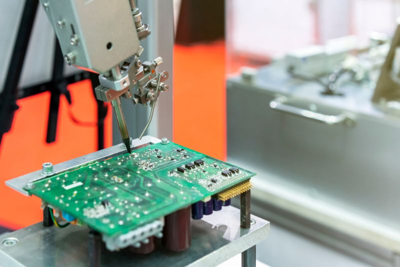
Assembly
This stage involves populating the PCB with electronic components like resistors, capacitors, and integrated circuits (ICs). Here’s a closer look:
- Component Placement: Precisely calibrated machines pick and place components onto designated pads on the PCB.
- Soldering: Components are permanently attached to the PCB using solder, which forms a strong electrical and mechanical connection. Special soldering techniques might be required to accommodate the flexible sections for flex-rigid PCBs.
- Testing: The assembled PCB undergoes rigorous electrical testing to ensure functionality and identify defects.
Each stage plays a critical role in ensuring a high-quality, functional PCB. Flaws at any stage can lead to costly rework or even complete board failure. Understanding each step allows designers and engineers to optimize their work for manufacturability, promoting a smooth and efficient production process.
Strategies For Optimizing PCB Manufacturing Processes
Optimizing PCB fabrication and assembly is akin to conducting a flawless symphony. Now that you have learned about every stage, from design to testing, adding a flow to your manufacturing process is essential, which helps you seamlessly achieve a high-quality, functional product.
Here, we explore key strategies to elevate your PCB manufacturing process:
Design for Manufacturability (DFM)
DFM principles are the foundation for efficient and cost-effective PCB fabrication and assembly. By adhering to these guidelines during the design stage, you can significantly reduce potential issues downstream. Here are some crucial DFM considerations:
- Trace Width and Spacing: Maintaining recommended trace widths and spacing ensures proper signal integrity and prevents unwanted electrical shorts during etching. IPC standards, such as IPC-2221, provide detailed guidelines for trace dimensions based on material thickness and current carrying capacity.
- Via Types and Placement: DFM dictates the selection of via types (through-hole, blind, buried) and their placement to optimize signal routing and manufacturability. For flex-rigid PCBs, via placement, it needs to consider potential stress points during bending. IPC standards like IPC-2223 offer valuable guidance on types and placement practices.
- Component Selection and Placement: Choosing standard, readily available components minimize procurement challenges and potential assembly issues. Component placement should also consider pick-and-place machine capabilities and minimize the risk of component damage during assembly.
- Panel Size and Fiducials: Optimizing panel size maximizes material utilization and minimizes waste. Strategically placed fiducials are reference points for automated machines during assembly, ensuring precise component placement.
Advanced Manufacturing Techniques
The PCB manufacturing landscape is constantly evolving, with new technologies pushing the boundaries of efficiency and precision:
- Laser Drilling: This technique utilizes lasers to create precise holes in PCB materials, including flex-rigid PCBs. Laser drilling offers cleaner cuts, minimizing stress on flexible sections and improving accuracy.
- Direct Imaging: This method eliminates the need for traditional photolithography, using lasers to directly define the circuit pattern onto the copper layer. Direct imaging offers faster turnaround times and potentially higher resolution for complex designs.
- Advanced Soldering Techniques: Selective soldering uses solder paste only on designated areas, reducing solder waste and minimizing thermal stress on components. This technique is particularly beneficial for flex-rigid PCBs, where controlling heat exposure is crucial for maintaining flexibility.
Collaboration and Communication
A seamless flow of information between designers, manufacturers, and assemblers is essential for optimizing PCB fabrication and assembly.
Early collaboration allows for identifying potential DFM issues early on, preventing costly rework and delays.
Open communication regarding material availability, manufacturability concerns, and assembly constraints fosters a collaborative environment that optimizes the entire process.
Continuous Improvement
The Plan-Do-Check-Act (PDCA) cycle is a powerful tool for continuous improvement in PCB manufacturing. Here’s a breakdown of each stage:
- Plan: Establish clear goals for process improvement, focusing on areas with potential for optimization.
- Do: Implement the planned changes in a controlled manner, potentially on a pilot basis for flex-rigid PCBs due to their complexities.
- Check: Evaluate the effectiveness of the implemented changes by monitoring key metrics like yield rate, cycle time, and defect rate.
- Act: Based on the evaluation, either standardize the successful changes or refine the plan for further improvement.
By adopting the PDCA cycle, PCB manufacturers can continuously identify and eliminate inefficiencies, leading to a more optimized and cost-effective production process.
Optimizing For Different Needs
The world of PCB manufacturing isn’t a one-size-fits-all environment. Process strategies need to adapt to cater to diverse project requirements. Here’s how we can optimize for different needs:
High-Volume vs. Low-Volume Production
- High-Volume: For high-volume PCB fabrication and assembly, priorities shift towards maximizing efficiency and minimizing costs. Panelization techniques that allow for multiple PCBs on a single panel become crucial for efficient material utilization. Standardized processes with minimal manual intervention ensure consistent quality and rapid turnaround times.
- Low-Volume: Low-volume production allows for more flexibility in process selection. Rapid prototyping techniques, like laser direct imaging, can be leveraged for faster turnaround times. Working with experienced manufacturers who specialize in handling these complexities is essential for low-volume flex-rigid PCBs.
Need for Speed vs. High-Precision Requirements
- Speed: When speed is paramount, techniques like direct imaging and selective soldering can expedite the PCB fabrication and assembly. However, these techniques might not be suitable for high-precision applications with stringent electrical requirements.
- High-Precision: For high-precision PCBs, meticulous attention is paid to detail during each stage. Advanced inspection techniques ensure tight tolerances and flawless circuit integrity. Laser drilling becomes especially important for flex-rigid PCBs to maintain precision via placement and minimize stress points.
Cost Optimization Strategies
Cost optimization is a constant pursuit in PCB manufacturing. Here are some key strategies:
- DFM Best Practices: Adherence to DFM principles throughout the design stage minimizes potential rework and scrap during fabrication and assembly, leading to significant cost savings.
- Material Selection: Choosing readily available and cost-effective materials while meeting performance requirements can positively impact the overall project cost.
- Standardized Processes: Streamlined and standardized processes minimize human error and rework, leading to cost savings and improved yield rates.
- Supplier Relationships: Building strong relationships with reputable PCB manufacturers can unlock cost benefits through volume discounts and potentially negotiated pricing on materials and processes, especially for flex-rigid PCBs due to their specialized nature.
By understanding these optimization strategies and tailoring them to specific project needs, you can achieve a balance between cost, speed, and precision in your PCB manufacturing process.
Environmental Considerations
PCB fabrication and assembly processes can have an environmental impact. Chemicals used in etching and plating can be hazardous if not disposed of responsibly. Additionally, lead-containing components and energy-intensive equipment contribute to environmental concerns.
Strategies for Sustainable PCB Production:
Fortunately, the industry is moving towards sustainable practices:
- Material Selection: Utilizing lead-free components and halogen-free flame retardants minimizes the presence of harmful toxins in PCBs. Exploring bio-based or recyclable materials for the flexible substrates of flex-rigid PCBs can further reduce the environmental footprint.
- Energy-efficient Equipment: Investing in energy-star certified equipment for PCB fabrication and assembly reduces overall power consumption and minimizes the environmental impact.
- Water Conservation Techniques: Recycling and reusing water during rinsing and cleaning stages can significantly reduce water usage. Additionally, exploring water-based cleaning solutions can further minimize environmental impact.
By adopting these sustainable practices, PCB manufacturers can contribute to a greener future while maintaining efficient production processes.
Conclusion: The Power of a Well-Composed Symphony
Optimizing PCB manufacturing is a continuous journey requiring a holistic approach. Here are the key takeaways:
- Embrace Design for Manufacturability (DFM) principles: A well-designed PCB, considering manufacturability from the outset, minimizes rework and waste during fabrication and assembly.
- Leverage Advanced Manufacturing Techniques: Techniques like laser drilling and direct imaging offer improved efficiency and precision, leading to a more optimized process.
- Foster Collaboration and Communication: Open communication between designers, manufacturers, and assemblers ensures early identification of potential issues and facilitates process optimization.
- Embrace Continuous Improvement (PDCA): Manufacturers can achieve a more efficient and cost-effective PCB production environment by constantly evaluating and refining processes.
- Consider Environmental Impact: Sustainable practices like material selection and water conservation techniques minimize the environmental footprint of PCB manufacturing.
By implementing these strategies, you can transform your PCB manufacturing process into a well-rewritten masterpiece, delivering high-quality products while ensuring efficiency, cost-effectiveness, and environmental responsibility.
Remember, optimizing for flex-rigid PCBs might require additional considerations due to their unique material properties and complexities. Working with experienced manufacturers specializing in these boards is crucial for achieving optimal results.
After reading this comprehensive report, we hope you’ll pave the way for a future where PCB manufacturing thrives in harmony with environmental responsibility.