In the realm of electronic manufacturing, PCB assembly and testing are crucial steps that ensure the successful creation of functional and reliable printed circuit boards (PCBs). This blog post will provide a comprehensive overview of PCB assembly and testing, emphasizing the importance of these processes in the realm of PCB manufacturing.
Understanding PCB Assembly
PCB assembly integrates electronic components onto a bare PCB to create a fully functional circuit board. It involves meticulous placement and soldering of various elements, allowing for the creation of electrical connections and circuits.
Overview of the Assembly Process:
The assembly process begins after the PCB has undergone fabrication and preparation. It involves several key stages, including component selection, soldering and mounting, and thorough quality control and inspection. Each step is critical in ensuring the successful assembly of the PCB.
Role of PCB Design in the Assembly Process:
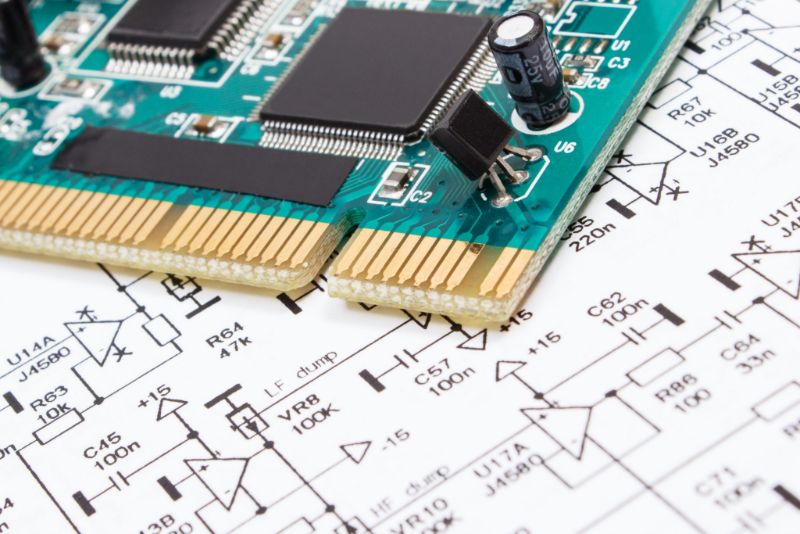
Efficient PCB design is paramount to the success of the assembly process. Factors such as component placement, trace routing, and adherence to design rules are considered during the design phase. A well-designed PCB facilitates a streamlined and error-free assembly process.
Importance of Choosing the Right Components for Assembly:
Selecting the appropriate components is vital to ensure optimal functionality and compatibility of the PCB. Component selection encompasses various considerations, including component specifications, quality, availability, and cost. High-quality components that meet design requirements are crucial for successful PCB assembly.
Key Steps in PCB Assembly
PCB Fabrication and Preparation:
The first step in the assembly process is PCB fabrication, where the bare PCB is created by etching copper traces, drilling holes, and preparing the PCB layers. Thorough cleaning and inspection of the fabricated PCB are essential to guarantee its quality and readiness for assembly.
Component Selection and Procurement:
Careful component selection is crucial to ensure the compatibility and reliability of the assembled PCB. Manufacturers must consider component specifications, availability, quality, and cost factors. By sourcing components from trusted suppliers, they can ensure a smooth and efficient assembly process.
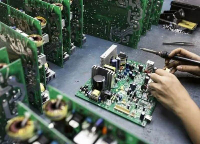
Soldering and Mounting Components:
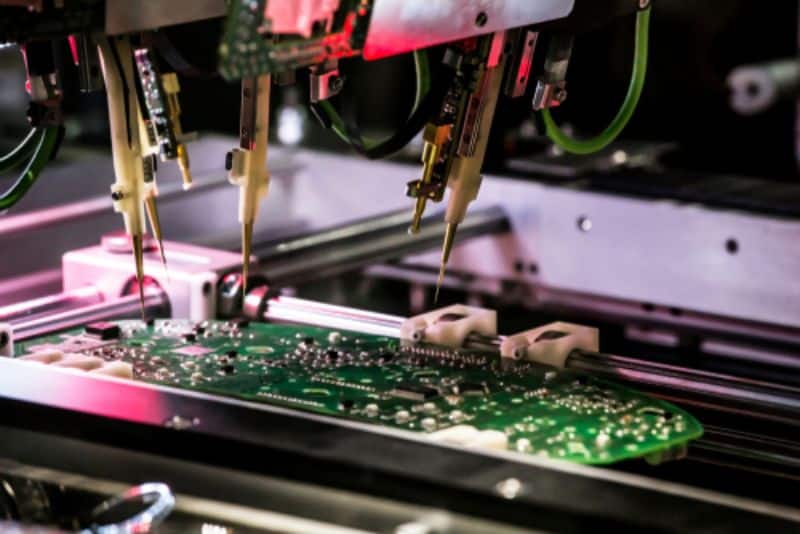
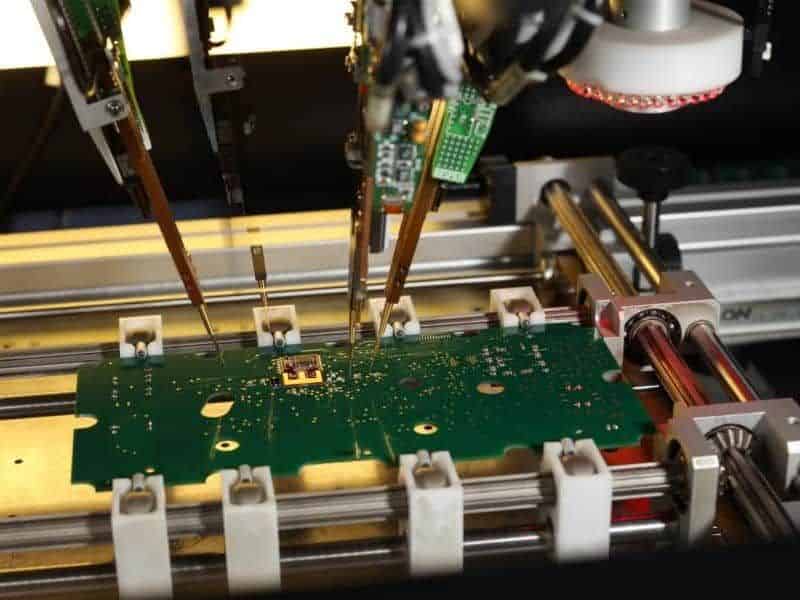
The soldering and mounting stage involves attaching the selected components onto the PCB. Through-hole assembly involves inserting component leads into pre-drilled holes and soldering them to the opposite side of the PCB. Surface Mount Technology (SMT) assembly, on the other hand, entails soldering smaller components directly onto the surface of the PCB. A mixed assembly combines both through-hole and SMT techniques based on design requirements.
Quality Control and Inspection:
Quality control and inspection are vital steps to verify the integrity and reliability of the assembled PCB. Visual inspection, automated optical inspection (AOI), and X-ray inspection techniques are employed to detect any defects or abnormalities in the soldering, component alignment, and overall assembly quality. Thorough testing ensures that the PCB meets the required specifications and standards.
Types of PCB Assembly Techniques
Through-Hole Assembly:
Through-hole assembly is a traditional technique where component leads are inserted through pre-drilled holes on the PCB and soldered to the opposite side. This technique offers robust mechanical connections and is suitable for larger components that require enhanced stability.
Surface Mount Technology (SMT) Assembly:
SMT assembly involves mounting smaller components directly onto the surface of the PCB. This technique offers increased component density, reduced PCB size, improved electrical performance, and compatibility with automated assembly processes.
Mixed Assembly (Combination of Through-Hole and SMT):
The mixed assembly utilizes a combination of both through-hole and SMT techniques, allowing for flexibility in component selection. It offers advantages in terms of design complexity, space optimization, and component availability.
Testing and Quality Assurance
Importance of Testing in PCB Assembly:
Testing is a critical phase in the PCB assembly process, ensuring that the assembled PCB functions as intended. It helps identify and rectify any manufacturing defects, component failures, or connectivity issues. Thorough testing significantly contributes to the reliability and performance of the final product.
Functional Testing Methods:
Functional testing involves evaluating the performance of the assembled PCB by subjecting it to various electrical tests. These tests verify the functionality of the circuit, such as checking for proper power distribution, signal integrity, and overall operational capabilities.
Automated Testing Techniques:
Automated testing techniques, including in-circuit testing (ICT) and flying probe testing, provide an efficient and accurate assessment of the assembled PCB. These techniques use specialized equipment to analyze the electrical characteristics and connectivity of the circuit, ensuring proper functionality.
Quality Control and Inspection Processes:
Quality control and inspection procedures are implemented throughout the assembly process to maintain high standards and ensure the reliability of the PCB. Automated optical inspection (AOI) systems detect defects in solder joints, component placement, and overall assembly quality. X-ray inspection helps identify hidden defects, such as solder bridging or insufficient soldering.
PCB Assembly Challenges and Solutions
Common challenges in PCB assembly
PCB assembly comes with its own unique set of challenges that manufacturers and assemblers often face. Let’s delve deeper into some common challenges and their corresponding solutions:
Component Compatibility Issues
Ensuring component compatibility is crucial for successful PCB assembly. Challenges may arise when integrating different components with varying specifications, such as voltage requirements, pin configurations, or form factors. To overcome this challenge, it is important to:
- Thoroughly review component datasheets and specifications to ensure compatibility with the PCB design.
- Collaborate with component suppliers to verify compatibility and seek their guidance in selecting appropriate components.
- Prototype and test the assembly to validate component compatibility before full-scale production.
Soldering and Joint Reliability Concerns
Achieving reliable solder joints is vital for the long-term performance and reliability of the PCB. Challenges in soldering and joint reliability can occur due to factors such as:
- Improper solder paste application.
- Inconsistent heating during the reflow process.
- Insufficient quality control measures.
To address these challenges, consider the following solutions:
- Implement stringent quality control measures throughout the assembly process, including automated optical inspection (AOI) or X-ray inspection to detect potential defects.
- Provide proper training to assemblers on soldering techniques and best practices to ensure consistent and reliable solder joints.
- Optimize the reflow profile, including temperature ramp-up, peak temperature, and cooling rate, to achieve optimal solder joint formation.
Thermal Management Challenges
With the increasing complexity and miniaturization of electronic devices, thermal management becomes a critical aspect of PCB assembly. Challenges may arise due to:
- Inadequate heat dissipation.
- Insufficient consideration of thermal factors during design.
To mitigate thermal management challenges, consider the following solutions:
- Strategically place heat-generating components on the PCB to optimize airflow and heat dissipation.
- Incorporate thermal vias, heat sinks, and thermal pads to efficiently transfer heat away from sensitive components.
- Perform thorough thermal testing and validation to ensure the PCB can withstand operating temperatures.
Software Tools for PCB Design and Assembly
Overview of software options for PCB design
Various software tools are available to aid in the PCB design and assembly process. Let’s explore some of the key software options in more detail:
Electronic Design Automation (EDA) Tools
EDA tools are widely used in PCB design and offer a comprehensive suite of features to streamline the design process. These tools typically include:
- Schematic capture: Allows designers to create circuit diagrams and specify component connections.
- PCB layout: Provides tools for placing components and routing traces on the PCB.
- Design rule checks (DRC): Checks the design against predefined manufacturing rules to ensure compliance.
Some popular EDA tools include Altium Designer, Cadence Allegro, and Mentor Graphics PADS.
Free software for PCB design and simulation
In addition to commercial software options, free tools are available for PCB design and simulation. These tools are often suitable for hobbyists, startups, or small-scale projects. Here are a few notable examples:
KiCad
KiCad is an open-source EDA tool that offers a complete PCB design suite. It includes schematic capture, a PCB layout, and a 3D viewer. KiCad has an active user community and frequent updates, making it a popular choice for those seeking free PCB design software.
EasyEDA
EasyEDA is a web-based EDA tool that allows users to design and simulate circuits online. It offers a user-friendly interface, cloud-based storage, and collaboration features. EasyEDA is a great option for beginners or those seeking a simple and accessible PCB design tool.
Tools for PCB layout and component placement
Efficient PCB layout and component placement are crucial for optimal performance and manufacturability. Here are some essential tools that can aid in these processes:
AutoCAD or DraftSight
CAD software tools like AutoCAD or DraftSight enable designers to create precise PCB layouts, define component footprints, and generate accurate manufacturing files. These tools provide advanced capabilities for creating complex and detailed PCB designs.
PCB Footprint Libraries
Component footprint libraries provide pre-defined component footprints, saving time and ensuring accurate placement during the design process. The IPC-7351 standard or manufacturer-specific libraries are commonly used to access various component footprints.
Design Rule Check (DRC) Software
DRC software verifies design compliance with manufacturing rules. It helps detect errors such as component overlaps, trace clearances, or solder mask issues. DRC functionality is often integrated into EDA tools or available as standalone applications.
Importance of design-for-manufacturability (DFM) considerations
Design-for-manufacturability (DFM) considerations are crucial for ensuring smooth and efficient PCB assembly. DFM involves designing PCBs with manufacturing and assembly processes in mind. Here’s why DFM is important:
Cost and Time Optimization
DFM practices can help minimize costly and time-consuming design iterations by considering manufacturing constraints early in the design process. This results in improved efficiency and reduced production delays.
Improving Manufacturing Yield
DFM practices help optimize the design for higher manufacturing yields. By considering manufacturing processes, such as component placement, trace routing, and panelization, designers can reduce the likelihood of errors, defects, or failures during assembly.
Enhancing Product Reliability
DFM practices contribute to improved product reliability. Designs that account for manufacturing processes and limitations can result in better quality control, fewer assembly-related issues, and longer product lifespans.
Best Practices for Successful PCB Assembly
Collaboration between PCB designers and assemblers
Successful PCB assembly relies on effective collaboration between PCB designers and assemblers. Here are some best practices to foster collaboration:
- Early Involvement: PCB assemblers should be involved in the design process from an early stage. This ensures that design decisions consider manufacturability and assembly requirements, reducing potential issues during production.
- Clear Communication Channels: Establish open lines of communication between designers and assemblers. Regular meetings, design reviews, and documentation exchange help clarify expectations, address concerns, and ensure alignment throughout the assembly process.
- Design for Assembly (DFA): Designers should implement DFA principles to simplify assembly and reduce the risk of errors. By considering assembly steps, accessibility, and component placement, designers can optimize the efficiency of the assembly process.
Effective communication and documentation
Clear communication and comprehensive documentation are crucial for successful PCB assembly. Consider the following best practices:
- Detailed Assembly Instructions: Provide detailed assembly instructions that clearly outline the assembly process, including component placement, soldering guidelines, and any specific handling instructions. This ensures consistency and minimizes the risk of errors.
- Bill of Materials (BOM): Maintain an accurate and up-to-date BOM that includes component specifications, part numbers, and sources. The BOM should also specify any special considerations, such as alternate part options or preferred suppliers. Having a comprehensive BOM helps streamline the procurement process and ensures the availability of the required materials for assembly.
- Design Documentation: Proper documentation is vital throughout the PCB assembly process. This includes schematic diagrams, PCB layouts, assembly drawings, and any design notes or annotations. The documentation should be well-organized, easily accessible, and regularly updated. It serves as a reference for assemblers, allowing them to understand the design intent, component placement, and any specific requirements or considerations. Clear and comprehensive design documentation promotes efficient communication between the design and assembly teams, resulting in smoother assembly processes and a higher likelihood of successful PCB assembly.
Attention to detail and precision during assembly
Attention to detail and precision during the assembly process is essential to ensure the quality and reliability of the final PCB. Consider the following best practices:
- Component Handling: Handle components with care to prevent damage or contamination. Use proper ESD (Electrostatic Discharge) protection measures to avoid static electricity damage, especially for sensitive components.
- Soldering Techniques: Follow industry-standard soldering techniques to ensure reliable connections. Use the appropriate soldering equipment, temperature settings, and solder types. Properly clean and inspect solder joints to identify and correct any defects.
- Component Placement and Orientation: Ensure accurate component placement and verify the correct orientation of components, especially for polarized components like capacitors or diodes. This helps avoid assembly issues and potential short circuits.
Implementing quality control and testing protocols
Implementing robust quality control measures and testing protocols is crucial for ensuring the functionality and reliability of the assembled PCB. Consider the following best practices:
- Automated Optical Inspection (AOI): Utilize AOI systems to automatically inspect the quality of solder joints, component placement, and overall assembly. AOI helps identify potential defects and ensures compliance with design specifications.
- In-Circuit Testing (ICT): Perform in-circuit testing to verify the functionality of the assembled PCB. ICT involves testing individual components and checking the connectivity of circuit paths to detect any faults or issues.
- Functional Testing: Conduct functional testing to ensure that the assembled PCB meets the intended performance and functionality requirements. This may involve subjecting the PCB to simulated real-world conditions or running specific tests to validate its performance.
Conclusion
PCB assembly is a critical process that requires attention to detail, effective collaboration, and the use of appropriate software tools. Overcoming challenges such as component compatibility, soldering reliability, and thermal management is essential for successful assembly. By following best practices, implementing robust quality control measures, and staying updated with emerging trends, manufacturers can ensure high-quality PCB assembly that meets the demands of the ever-evolving electronics industry.
Looking ahead, the future of PCB assembly is marked by advancements in miniaturization, the increasing demand for flexible and rigid-flex PCBs, and the impact of emerging technologies. As electronic devices become smaller and more complex, PCB assembly must adapt to accommodate these trends. Industry professionals must stay proactive, embrace innovation, and strive for excellence in PCB assembly to drive advancements and deliver reliable and efficient electronic products. By doing so, they can contribute to the growth and success of the electronics industry and meet the needs of a rapidly changing world.