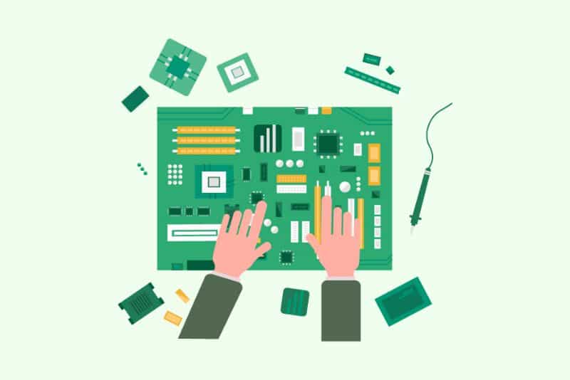
Imagine a world without the marvels of modern technology – a world devoid of smartphones, laptops, medical devices, and smart appliances. All of these incredible innovations share a common silent hero: the Printed Circuit Board, or PCB. These unassuming platforms of interconnected electronic components are the backbone of today’s electronics, orchestrating the symphony of signals that power our lives.
But here’s the catch: while PCBs might seem like magic, designing them requires a wizard’s touch – a touch that knows how to dance between components, weave intricate traces, and orchestrate symphonies of signals. Enter the realm of PCB design, where every element counts, every connection matters, and every misstep can result in a catastrophic design failure.
In this voyage of discovery, we’ll navigate through the treacherous waters of PCB design, uncovering the top 10 mistakes that can transform even the most promising designs into a labyrinth of glitches and frustrations. But don’t worry – we won’t leave you adrift. With each pitfall, we’ll also offer insights into how to navigate these challenges and set sail toward successful PCB designs.
Whether you’re a seasoned designer seeking to refine your craft or a newcomer stepping into the world of electronics, this blog is your compass for steering clear of design pitfalls and embracing the art of designing flawless PCBs. So, fasten your seatbelts and prepare to embark on a journey where every trace, every connection, and every decision counts. Welcome to the realm of PCB design mastery – where precision and innovation shape the future of electronics.
Understanding PCBs and Their Design Process
What is a PCB?
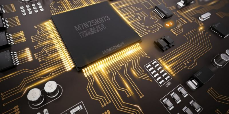
At its core, a Printed Circuit Board (PCB) is a flat board made of non-conductive material, often fiberglass, with conductive pathways etched onto its surface. These pathways, or traces, connect various electronic components, forming the intricate web that enables devices to function as intended.
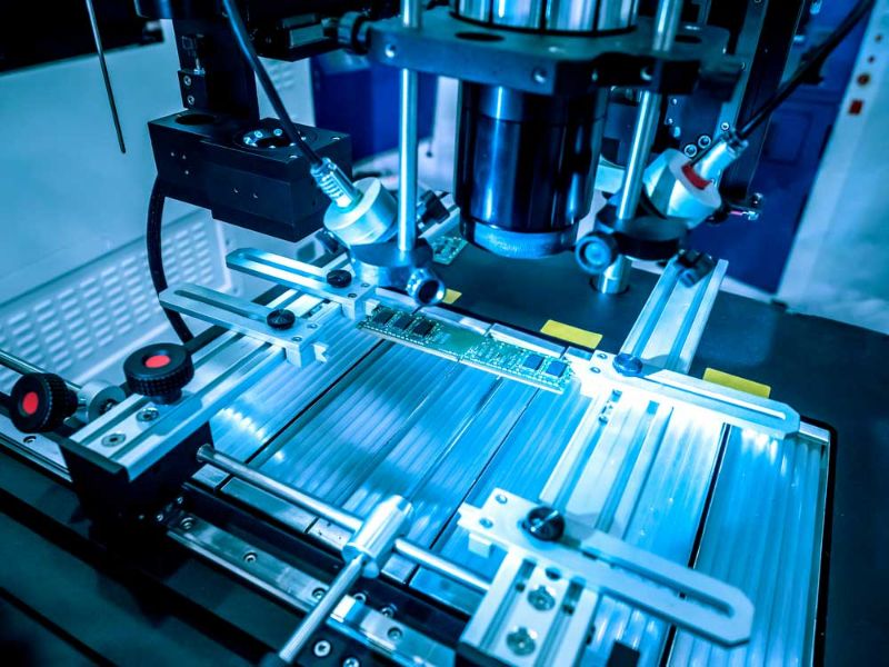
PCB Design Process Overview
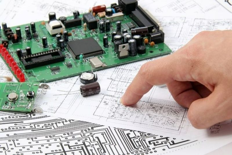
The creation of a PCB involves multiple stages, from conceptualizing the circuit’s functionality to realizing it in a physical layout. It begins with schematic design, where designers define the connections and components’ relationships. This schematic is then translated into the actual physical layout using specialized software. Components’ placement, routing of traces, and consideration of power planes all come into play at this stage.
Collaboration between designers, engineers, and manufacturers is crucial. Engineers provide expertise in component selection and circuit functionality, while manufacturers offer insights into the production process’s practicalities.
Importance of Effective PCB Design
A well-designed PCB is the backbone of electronic devices, ensuring optimal performance, reliability, and cost-efficiency. Design mistakes can lead to manufacturing delays, costly rework, and even catastrophic failures in the field. Embracing a meticulous design approach minimizes these risks and delivers superior products.
Benefits of a Well-Designed PCB
Optimal Signal Integrity
A well-designed PCB is a symphony of precision, and one of its most vital aspects is maintaining optimal signal integrity. Signal paths must be meticulously crafted to minimize distortion and interference, ensuring that data flows smoothly between components.
In the realm of PCB layouting, meticulous trace routing is paramount. The intricacies of routing, such as trace length matching and impedance control, significantly impact signal quality. Adequate separation between analog and digital traces prevents unwanted coupling that could degrade signals.
Efficient Power Distribution
Power distribution across a PCB is a critical aspect that requires careful consideration. A well-designed PCB ensures even power distribution to all components, preventing some from being starved of power while others are overloaded.
In the world of PCB manufacturing companies, the distribution of power and ground planes is strategically planned. Decoupling capacitors are positioned close to power pins to filter out noise. This meticulous distribution avoids voltage drops, ensuring consistent power delivery throughout the board.
Thermal Management
Efficient thermal management is essential for maintaining the longevity and reliability of electronic components. Heat is the enemy of electronics, and a well-designed PCB incorporates strategies to dissipate heat effectively.
In PCB design, this involves strategically placing heat-generating components on the board and ensuring proper airflow. Additionally, thermal vias can be used to conduct heat away from hotspots. Manufacturers in PCB production use techniques such as heat sinks, thermal pads, and even active cooling solutions for critical components.
Common Mistakes in Your PCB Design
Insufficient Clearances and Spacing
Amid the race to fit an increasing number of components onto smaller PCBs, overlooking adequate clearances between traces, pads, and components can lead to shorts and erratic behavior. This is a common oversight in the realm of PCB design that can hamper the final product’s performance. Overlooking spacing requirements can result in unintended electrical connections, jeopardizing the reliability of the entire board.
It’s crucial to adhere to industry standards for minimum clearances and spacing to avoid falling into this pitfall. Furthermore, it’s important to factor in the potential for temperature variations that could cause the expansion and contraction of materials, potentially affecting the distances between components.
Ignoring Signal Integrity
The importance of signal integrity cannot be overstated in PCB design and PCB manufacturing. A fundamental aspect of ensuring a well-functioning PCB is maintaining signals’ integrity as they traverse the board. Ignoring this consideration can lead to a host of issues, from signal degradation to susceptibility to noise.
By prioritizing signal integrity, designers must engage in meticulous trace routing. This involves careful planning of signal paths, avoiding sharp bends, and implementing differential pair routing for high-speed signals. Also, proper grounding techniques should be employed to minimize noise and crosstalk, ensuring the final product performs as intended.
Component Placement Errors
The strategic placement of components holds the key to optimal PCB layout and performance. Overlooking the significance of component placement can lead to compromised functionality, signal integrity, and even thermal management.
In the world of PCB manufacturing, proper PCB assembling hinges on well-thought-out component placement. Designers should give meticulous attention to component orientation, ensuring they’re correctly positioned for optimal heat dissipation. Grouping related components together not only aids in thermal management but also streamlines the signal path, enhancing overall performance. Moreover, ensuring adequate spacing for accessibility and maintenance eases the serviceability of the end product.
Manufacturing Constraints and Challenges
Design for Manufacturability (DFM)
Designing a PCB isn’t just about creating an aesthetically pleasing layout; it’s also about ensuring that the design can be efficiently manufactured. This is where the concept of Design for Manufacturability (DFM) comes into play.
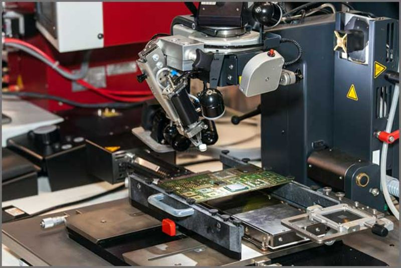
Manufacturers, whether they are PCB manufacturing companies or individual PCB manufacturers, have specific capabilities and limitations. A well-designed PCB takes these factors into account. Overlooking DFM can lead to unnecessary complications during production, such as difficulty in soldering components, insufficient clearances for automated assembly machines, and more. Collaborating closely with manufacturers to understand their processes and constraints is crucial to creating a design that can be smoothly transformed into a physical product.
Neglecting Testing and Validation
Testing and validation are one of the most critical phases in the journey from PCB design to a functional product. Unfortunately, it’s also a phase that can be easily overlooked or rushed through.
In the realm of PCB layouting, this can translate to failing to incorporate test points and access for probes, making testing the board’s functionality challenging. In the world of PCB manufacturing, neglecting comprehensive testing can result in faulty boards reaching customers, leading to dissatisfaction and costly recalls.
Effective testing strategies encompass both functional and performance testing. Components’ values, placements, and orientations should be meticulously reviewed. Simulation tools can be used to validate the design before it enters production, ensuring that the board behaves as intended. Collaborating with experienced engineers and incorporating their feedback during the testing phase is a prudent approach.
Top 10 Mistakes in Your PCB Design to Avoid
Inadequate Clearances and Spacing
Within the intricate landscape of PCB design, where every component’s placement and connection count, overlooking clearances and spacing can lead to a cascade of issues. It’s more than just preventing a jumble of components; it’s about safeguarding against electrical malfunctions. Take a deep dive into the importance of adhering to manufacturer-recommended clearances and spacing guidelines. Explain how improper spacing can result in unintended electrical connections, leading to short circuits and even catastrophic failures. Emphasize the need to consider the physical dimensions of components and traces while also accommodating for manufacturing tolerances.
Poor Routing Practices
Imagine a city without proper roads – chaos and confusion would ensue. The same applies to PCBs. Poor routing practices can lead to a cacophony of signal integrity issues, like crosstalk and impedance mismatches. Paint a picture of how meticulous trace routing is akin to orchestrating a symphony, where the harmonious arrangement of traces leads to optimal performance. Highlight the significance of following proper routing techniques, from adhering to impedance-controlled traces for high-speed signals to minimizing trace lengths to prevent signal degradation. Dive into how advanced routing algorithms and tools can help designers avoid pitfalls and achieve signal integrity nirvana.
Component Placement Challenges
The art of component placement goes beyond aesthetics; it’s about orchestrating a symphony of functionality and thermal management. Delve deep into the intricacies of strategic component placement. Describe how placing components too close can lead to thermal coupling, where heat-generating components affect their sensitive counterparts. Explore the dance of separating analog and digital components to minimize interference. Elaborate on the role of thermal vias, which act as pathways for heat dissipation, and how their strategic placement is crucial for preventing hotspots.
Neglecting Power Distribution
Picture an electrical grid – it powers an entire city. Similarly, a well-designed power distribution network powers an entire PCB. Diving into the realm of power distribution, elaborate on the intricacies of planning power and ground planes. Discuss the significance of decoupling capacitors, strategically placed to stabilize power delivery. Detail the implications of inadequate voltage drops and the potential for erratic behavior. Use real-world examples to showcase how meticulous power distribution design can prevent a chain reaction of problems.
Disregarding Thermal Considerations
Heat is the natural byproduct of functionality, but unchecked heat can lead to a PCB meltdown. Plunge into the depths of thermal considerations, explaining how inadequate thermal management can result in components operating outside their temperature limits. Delve into the art of proper heat sinking, from selecting the right materials to ensuring sufficient contact area for efficient heat dissipation. Explore advanced techniques like integrating heat pipes or even liquid cooling for components with high thermal dissipation demands.
Not Considering Manufacturing Constraints
Designing a PCB isn’t just about artistic expression; it’s a marriage of design and manufacturability. Delve into how designing for manufacturability is a strategic move that ensures the design can be seamlessly transformed into a physical board. Discuss how considering manufacturing constraints early in the design process can prevent design elements that are challenging or costly to produce. Highlight the importance of panelization – arranging multiple PCB designs on a single panel for cost-effective production. Paint a vivid picture of how designers collaborate closely with PCB manufacturing companies to ensure that the design is manufacturable and cost-efficient.
Overlooking Design Rule Checks (DRC)
Design Rule Checks (DRC) are the unsung heroes of PCB design, the diligent guardians against design errors. Dive into how these checks are critical in the design journey, catching issues like trace width violations, clearance violations, and unconnected nets. Explain how DRC ensures that the design adheres to manufacturer-specific guidelines and industry standards. Explore the consequences of disregarding DRC results – from non-functional boards to unreliable products – and highlight the role of DRC tools in preventing these mishaps.
Neglecting EMI/EMC Considerations
In the realm of electronics, where devices interact with one another, electromagnetic interference (EMI) and electromagnetic compatibility (EMC) are vital considerations. Transport readers into a world where unmanaged EMI leads to signal disruptions, malfunctions, and cross-device interference. Discuss how addressing EMI/EMC issues involves careful planning of signal paths, shielding sensitive components, and applying proper grounding techniques. Showcase real-world examples where overlooking EMI/EMC considerations resulted in costly redesigns and delayed projects.
Underestimating Testing and Validation
Testing and validation – the crucible where designs are truly put to the test. Plunge into the importance of creating prototypes for rigorous testing and design validation. From functional testing to signal integrity analysis, paint a vivid picture of how each testing phase ensures that the design performs as intended. Discuss the consequences of skipping testing phases, which can lead to unexpected issues in the final product, costly recalls, and even damage to reputation. Use anecdotes and case studies to illustrate the power of comprehensive testing.
Insufficient Documentation
Clear and comprehensive documentation is the torch that lights the path from design to manufacturing and beyond. In this section, embark on a journey through the intricate world of documentation. Highlight the importance of detailed schematics, thorough bill of materials (BOM), and comprehensive assembly instructions. Explain how these documents serve as a common language between designers, engineers, and manufacturers, ensuring that the design intent is accurately translated into a physical product. Discuss the risks of inadequate documentation, from miscommunication during manufacturing to challenges in troubleshooting and maintenance.
Conclusion
The journey through the top 10 PCB design mistakes has uncovered many insights for creating flawless designs. Summarize the key takeaways, from the critical role of proper spacing to the necessity of comprehensive documentation. Reinforce the idea that meticulous PCB design leads to devices that function as intended and endure the test of time.
Encourage readers to apply these insights to their own PCB design projects, ensuring that their creations rise above common pitfalls and contribute to the realm of electronics with optimal performance, reliability, and cost-effectiveness.