Printed Circuit Boards (PCBs) are the backbone of modern electronics, serving as the foundation for the assembly and connection of electronics PCB. Ensuring the quality and reliability of PCBs is crucial for properly functioning electronic devices, systems, and equipment. PCB testing and inspection are vital in identifying and rectifying defects and potential failures during the PCB creation process. This comprehensive guide will explore the best methods for PCB design, testing, and inspection, providing insights into various techniques, standards, and future trends.
Pre-Testing Preparations
Before delving into the testing and inspection methods, thorough preparations are essential to set the stage for successful PCB evaluation. This section covers the initial steps involved in preparing for the testing process.
Understanding the PCB Design and Fabrication
The first step in preparing for PCB design and testing is gaining a comprehensive understanding of the PCB design and the fabrication of PCB. This involves a detailed review of the schematic and a thorough analysis of the PCB layout. Engineers and technicians should carefully inspect the design to identify potential issues that may affect the functionality and reliability of the final product.
Schematic Review
The schematic is the blueprint of the PCB, illustrating the interconnections and relationships between components. During the schematic review, engineers verify the accuracy of the connections, check for potential signal integrity issues, and ensure that the design adheres to the intended functionality.
Layout Analysis
The PCB layout is critical in ensuring the efficient flow of electrical signals and power distribution. Analyzing the layout involves verifying the component placements, trace routing, and ground planes to identify potential design flaws that may lead to signal interference or thermal issues.
Components Verification
The quality and reliability of the components used in the PCB significantly impact the overall performance of the electronic device. As such, rigorous verification of the components is essential.
Bill of Materials (BOM) Check
A thorough review of the Bill of Materials (BOM) is necessary to ensure the correct components are specified and available for the PCB creator. This step helps prevent potential delays and ensures all components meet the required specifications.
Component Sourcing and Quality
Once the BOM check is complete, sourcing components from reputable suppliers is essential. Quality components significantly contribute to the longevity and reliability of the final product. Ensuring that components meet industry standards and reliability requirements is vital in avoiding premature failures.
Non-Invasive Testing Methods
Non-invasive testing methods allow inspection without damaging the PCB. These techniques help identify potential defects and anomalies on the surface and within the PCB assembly.
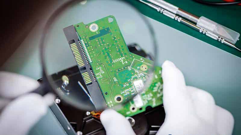
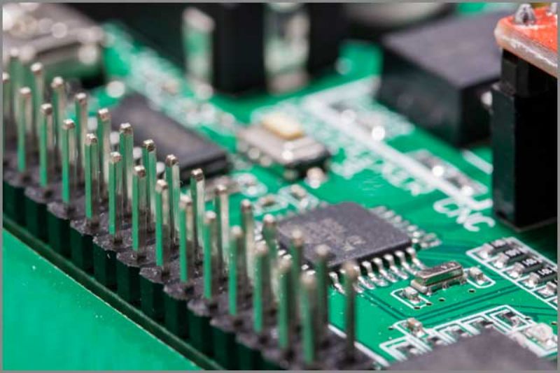
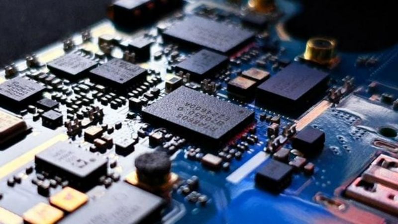
Visual Inspection
Visual inspection is one of the simplest and most effective non-invasive testing methods for electronics PCB. Trained inspectors visually examine the PCB for physical defects and irregularities, such as soldering issues, component misalignment, and PCB surface contamination.
Importance of Visual Inspection in Identifying Physical Defects
Visual inspection allows inspectors to identify defects that may affect the functionality and reliability of the PCB. Examples include solder bridges, lifted leads, and missing components.
Types of Defects Detected through Visual Inspection
Visual inspection can detect various defects, including those that are difficult to identify through automated methods. These defects may include solder splatters, solder voids, and improper component orientation.
X-ray Inspection
X-ray inspection is a powerful non-destructive testing technique that provides a detailed view of the internal structure of the PCB assembly. X-rays can penetrate the PCB to reveal hidden defects, such as insufficient solder joints and voids, without damaging the components or PCB layout.
How X-ray Inspection Reveals Hidden Defects
X-ray inspection allows inspectors to visualize internal connections and solder joints, helping to identify defects that are not visible from the surface. It is particularly useful for BGA (Ball Grid Array) components and complex multi-layer PCBs.
Ensuring the Integrity of Solder Joints with X-ray Inspection
X-ray inspection ensures that solder joints are free from defects such as cracks, voids, or insufficient solder, which can lead to electrical and mechanical failures.
In-Circuit Testing (ICT)
In-Circuit Testing (ICT) is a widely used automated testing method that checks the functionality of individual components and interconnections on the PCB. It is performed without applying power to the entire circuit.
Introduction to In-Circuit Testing and Its Benefits
ICT is a fast and efficient testing method that helps identify component failures, open circuits, and short circuits on the PCB.
Implementing In-Circuit Testing for Efficient Fault Detection
ICT is ideal for high-volume PCB design, as it can quickly detect defects and streamline the testing process.
Invasive Testing Methods
Invasive testing methods involve physically testing the PCB and its components, which may require some level of disassembly. These methods provide more in-depth insights into the electrical characteristics and performance of the PCB.
Solderability Testing
Solderability testing assesses the ability of the PCB’s surface and components to accept solder during assembly. Ensuring proper solderability is crucial for establishing reliable electrical connections.
Evaluating the Suitability of Soldering Materials and Processes
Solderability testing determines whether the chosen solder and soldering process is suitable for the specific PCB type materials and components.
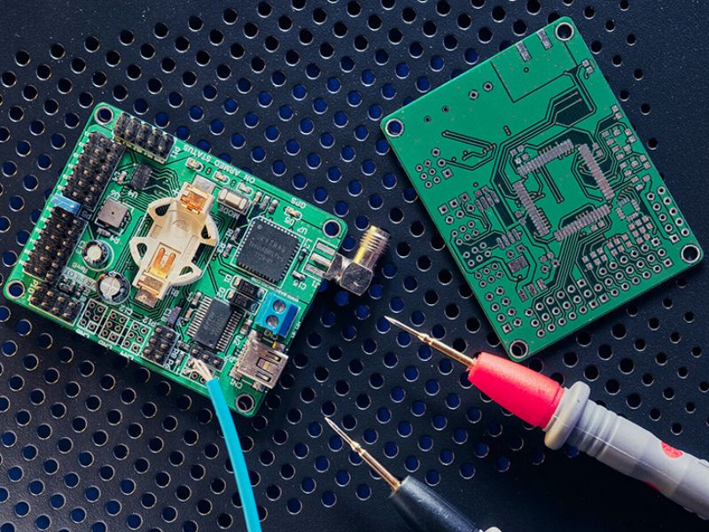
Electrical Testing
Electrical testing assesses the electrical performance of the PCB, ensuring that it meets design specifications and functions as intended.
Bare Board Testing
Bare board testing examines the electrical connectivity of the PCB before any components are soldered onto it.
Understanding the Significance of Bare Board Testing
Bare board testing is essential for identifying defects or issues related to the PCB creation process, such as open circuits or short circuits.
How Bare Board Testing Helps in Identifying Manufacturing Defects
By detecting manufacturing defects early in the production process, bare board testing minimizes the risk of further costly issues during assembly.
Flying Probe Testing
Flying probe testing employs a flying probe system to make contact with test points on the PCB, facilitating the evaluation of individual components and connections.
Advantages of Flying Probe Testing over Traditional Test Methods
Flying probe testing offers a flexible and cost-effective solution for low to mid-volume PCB design and can adapt quickly to design changes.
Overcoming Challenges and Limitations in Flying Probe Testing
While efficient for certain PCBs, flying probe testing may be slower for densely populated boards, making it essential to consider other testing methods.
Boundary Scan Testing (JTAG)
Based on the Joint Test Action Group (JTAG) standard, boundary scan testing is a powerful technique for testing complex digital circuits and interconnections.
Explaining Boundary Scan Testing and Its Role in PCB Inspection
Boundary scan testing uses dedicated test circuitry embedded within integrated circuits to verify their functionality and detect faults.
Interpreting Boundary Scan Test Results and Debugging
Interpreting the results of boundary scan tests can help identify faults and streamline the debugging process during PCB development.
Advanced Testing Techniques
Advanced testing techniques leverage sophisticated technologies and methodologies to ensure a comprehensive evaluation of the PCB’s functionality and performance.
In-Circuit Serial Programming (ICSP)
In-Circuit Serial Programming (ICSP) is a testing method that allows for the programming and testing of microcontrollers and other programmable components while they are still soldered to the PCB.
How ICSP Enhances PCB Testing and Programming
ICSP streamlines the programming process for mass-produced PCB layout, eliminating the need for manual programming, and saving time and effort.
In-Circuit Emulation (ICE)
In-Circuit Emulation (ICE) is an advanced testing technique that involves the use of an emulator to test and debug the PCB in real-time, providing valuable insights into the system’s behavior.
Real-Time Debugging with In-Circuit Emulation
ICE enables engineers to monitor and modify the system’s operation during the testing phase, making it easier to identify and resolve complex issues.
Thermal Imaging
Thermal imaging, also known as infrared thermography, is a non-destructive testing method that detects heat variations on the PCB, helping to identify hotspots and potential thermal issues.
Using Thermal Imaging for Overheating Detection
Thermal imaging is particularly useful for PCBs in power electronics and high-performance applications, where thermal management is critical.
Microsection Analysis
Microsection analysis involves the examination of cross-sectional samples of the PCB, allowing engineers to inspect internal structures and detect defects that may not be visible from the surface.
Identifying Internal Defects with Microsection Analysis
Microsection analysis helps identify issues such as delamination, voids, and cracks that may occur during the PCB manufacturing process.
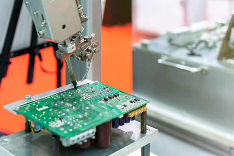
Importance of Automated Testing
Automated testing plays a vital role in PCB testing and inspection, enabling faster and more accurate evaluation of PCBs.
Benefits of Automated Testing
Improved Testing Efficiency and Throughput
Automated testing significantly reduces testing time, enabling higher production throughput and faster time-to-market.
Consistent and Repeatable Results
Automated testing ensures consistent testing conditions, reducing variability and improving result reliability.
Choosing the Right Testing Equipment
Selecting appropriate automated testing equipment is crucial for successful PCB design testing and inspection.
Key Considerations for Choosing Testing Equipment
Factors such as testing speed, flexibility, and compatibility with various PCB designs should be taken into account.
Design for Testability (DFT) Guidelines
Design for Testability (DFT) involves implementing design practices that make PCB testing and inspection more effective and efficient.
DFT Best Practices
Test Point Accessibility
Designing PCBs with accessible test points simplifies the testing process and reduces the need for specialized testing fixtures.
Boundary Scan (JTAG) Integration
Integrating boundary scan capabilities into the PCB design enhances testability, allowing for more thorough testing of digital components.
How DFT Improves Testing and Inspection Efficiency
DFT reduces test time, lowers testing costs, and improves fault coverage, making it an essential aspect of modern PCB design.
PCB Inspection and Quality Standards
Compliance with industry standards ensures the quality and reliability of the PCBs.
IPC-A-600 and IPC-A-610
IPC-A-600 provides acceptance criteria for PCBs, while IPC-A-610 defines the acceptance criteria for electronic assemblies.
RoHS Compliance and Lead-Free Assembly
Adhering to RoHS regulations and adopting lead-free assembly processes is crucial for environmental and health considerations.
Common PCB Defects and Failure Analysis
Understanding common PCB defects helps in improving testing and inspection processes.
Soldering Issues
Solder Bridging
Solder bridging occurs when two adjacent solder connections create an unintended electrical connection.
Solder Tombstoning
Solder tombstoning is when one end of a surface-mounted component lifts off the PCB during soldering.
Electrical Shorts and Opens
Electrical Shorts
Electrical shorts occur when two or more conductive elements unintentionally connect, causing a disruption in the circuit.
Electrical Opens
Electrical opens are interruptions in the circuit caused by broken or disconnected conductive elements.
Component Placement Errors
Misalignment or incorrect placement of components can lead to functional issues and reliability problems.
PCB Testing and Inspection in Mass Production
Maintaining quality control during mass production is critical for consistent PCB layout performance.
Quality Control in Manufacturing
Implementing strict quality control measures at various stages of production ensures that all PCBs meet the required standards.
Statistical Process Control (SPC)
Using SPC helps monitor and control the production process, ensuring that the output remains within acceptable limits.
PCB Testing for Different Applications
Different applications have specific requirements for PCB testing and inspection.
PCB Testing in Consumer Electronics
High-Volume Production
Consumer electronics often require high-volume production, demanding efficient testing methods.
Reliability and Durability
Ensuring the reliability and durability of PCBs is crucial for consumer electronics that experience frequent use.
PCB Testing for Automotive Applications
Temperature and Vibration Resistance
PCBs for automotive applications need to withstand extreme temperature variations and mechanical stress.
Safety and Reliability
Reliable PCBs are essential for critical automotive systems, such as airbags and braking systems.
Aerospace and Military PCB Testing
Harsh Environments
Aerospace and military applications demand PCBs that can operate reliably in extreme environments.
Stringent Testing and Compliance
PCBs for aerospace and military applications must adhere to strict testing and compliance standards.
Future Trends in PCB Testing and Inspection
Advancements in technology will shape the future of PCB testing and inspection.
Industry 4.0 and Smart Testing
The integration of smart technologies and data analytics will revolutionize the testing process.
Artificial Intelligence (AI) in PCB Testing
AI-driven algorithms will enhance fault detection and optimize testing procedures.
Conclusion
Thorough testing and inspection are critical for ensuring the quality, reliability, and performance of PCBs in electronic devices. By implementing the best methods for PCB design testing and adhering to industry standards, manufacturers can deliver superior products that meet the demands of modern technology. As technology continues to evolve, embracing innovative testing techniques and future trends will be key to staying at the forefront of PCB testing and inspection.