Take a look at freelancing websites like Upwork and Fiver, and you’ll find plenty of PCB designers who offer PCB layout and Gerber file preparation services. If you want to take your new board over to a fabricator to produce at high volume, you’ll need to give them much more than Gerber files and your PCB layout. Professional fabrication and assembly services need a full package of PCB manufacturing files to create your next circuit board at volume.
Cheap manufacturers will give you a bare board from your Gerber files without any further checks into your PCB layout or manufacturing files. When you work with the right manufacturing service and a professional design firm, you’ll get a complete set of files that have been thoroughly checked for accuracy. Not all manufacturers will generate these files for you, and you’ll need to deliver a set of files alongside your PCB layout data. Here’s what goes into your PCB manufacturing documentation and what you should expect from an experienced design team.
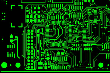
PCB Manufacturing Files Are More Than Gerber Files
If you look at most manufacturer websites, particularly quick-turn manufacturers that target the maker community, they usually reference creation of Gerber files and not much else. Today’s CAD tools can generate Gerber files with the click of a mouse button, but you won’t be able to edit them without other CAM tools (Numerical’s FAB3000 software is a great Gerber editor). If you talk to a PCB manufacturer, they will require much more than just Gerber files, especially if you need fully-assembled boards with more than 2 layers.
PCB manufacturers can’t work directly from your PCB layout files during fabrication; it’s simply too unwieldy and your PCB layout files don’t translate directly into fabrication instructions for automated equipment. Most fabricators will require some or all of the following PCB manufacturing files:
- Gerber files in specific formats. Your PCB Gerber files are used in lithography plotting machines to expose the etch resist on your bare board. Your fabricator should accept Gerber files in the RS-274-X format or the newer X2 format. Don’t forget to include an aperture file with your Gerber package.
- Netlist. This details all connections on the board in ASCII format. Together with your Gerber files, a netlist can be used to recreate your PCB layout, and it’s used to define nodes and connections in SPICE simulations.
- Fabrication drawings. These drawings show how the board stack-up is created. Layers need to be displayed in sequence (from top to bottom) so that there is no ambiguity in the layer order. Each layer is just a copy of the Gerber file for that layer. This file should also include a side-view of the stack-up.
- Assembly drawings. These drawings show where components will sit on the board. This document should show silkscreen information/component outlines with reference designators.
- Drill drawing. You drill drawing is normally included in your fabrication drawings on its own page. This will show where different drill hits will be applied, as well as a drill table showing the diameter of each drill hit. If you’re only using through-holes, then your drill drawing will just show a single layer.
- Backdrill and blind/buried via information. If you’re using blind/buried vias, you will need to delineate drill information by layer. In addition, if you’re using backdrilling for vias on high speed signals, backdrilled vias will need to appear in their own drill table with drilling depth so that your fabricator can setup their CNC equipment.
- Bill of materials. Your bill of materials needs to include several pieces of information beyond just a list of components. A complete bill of materials should include the reference designator, component manufacturer, distributor, and a short description. Note that, if you followed best practices for sourcing components, then you’ve already looked at the supply chain and determined available component stocks.
- PCB panel drawings. If you’re producing multiple boards, your fabrication drawings will need to show the panelized board. The Gerber files will also need to show an entire panel, not just an individual board. Your panelized drawings will also need to include routing and cutout instructions with dimensions.
- Any other fabrication notes. Critical notes regarding fabrication processes should be placed in the fabrication drawings. Other important notes required for your PCB manufacturer, such as firmware flashing instructions, should be placed in a separate documentation file.

Some fabricators will generate some or all of these files for your and will build these services into their costs. They will also charge you a non-recurring engineering (NRE) cost on top of any file creation costs. One fabricator I know will only ask for design files when quoting or starting a new job, probably because too many designers have made multiple mistakes when preparing their files. Other fabricators will give you a long list of PCB manufacturing files they’ll need in order to put your board into production.
Your Design Firm Can Help You With PCB Manufacturing Files
If you want to avoid creating incorrect PCB manufacturing files, you should work with an experienced design firm to help guide you through the PCB manufacturing process. The best design firms should go beyond creating your PCB layout and can help you with a number of other services:
- PCB layout checks. This is primarily an electrical check that looks for problems which may not be caught by all DRC engines. This also includes footprint checks, routing and signal integrity checks, and any other checks against your design requirements.
- DFM checks. It’s important to know that electrically correct design decisions may not be manufacturable. DFM checks are meant to spot these and other errors.
- Complete PCB manufacturing files preparation. Your design firm should know how to prepare the PCB manufacturing files presented above.
- Manufacturing management. When your PCB design firm has relationships with large and small manufacturers, they can help you get into production quickly and can manage the process for you.
The experienced PCB design and layout team at PCBLOOP can help you with your next advanced PCB layout and get your next board into production with a complete package of PCB manufacturing files. We help our clients stay at the cutting edge with advanced PCB design and layout services. We’ve also partnered directly with EDA companies and advanced PCB manufacturers, and we’ll make sure your next design is fully manufacturable at scale. Contact PCBLOOP for a consultation.
this article is great
Thank you for your comments