wThe world of technology is a canvas where innovation paints its wonders, and at the heart of this canvas are Printed Circuit Boards (PCBs). These unassuming yet remarkable creations are the architects of modern electronics, weaving a tapestry of connections that bring devices to life. Join us on a journey as we unveil the hidden treasures of PCBs and explore why a customized version is not just an option but a necessity in the realm of electronics manufacturing companies.
Understanding PCB Fabrication and Layout
What is a PCB Fabrication and Layout?
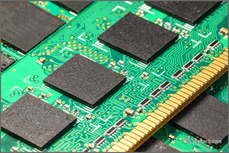
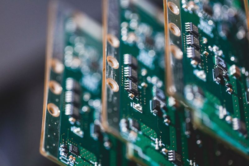
Think of a PCB as a conductor orchestrating the flow of electrons, akin to a symphony conductor directing musicians. It’s a board with a mission—a mission to connect components and enable devices to perform tasks that were once considered magic. PCB fabrication, often provided by reputable circuit board manufacturers, allows us to communicate, compute, and create with astonishing ease.
Importance of PCB Fabrication and Layout
To truly comprehend the significance of PCB fabrication and layout, envision a world without them—a world where wires crisscross like a tangled web, and each electronic device is a puzzle waiting to be solved. PCBs lay the foundation for order in this chaos. They’re the reason we have devices that function seamlessly, from handheld gadgets to colossal machines that power industries.
PCB Benefits
Compact Design and Space Efficiency
Modern electronic devices are becoming increasingly compact, yet their functionality continues to expand. This demand for miniaturization has led to the widespread adoption of Printed Circuit Boards (PCBs) and their meticulous layout due to their ability to accommodate intricate circuitry within limited spaces. PCB fabrication, often involving skilled engineers and precise manufacturing techniques, enables designers to create complex circuits that seamlessly fit into the smallest of enclosures. This compactness has revolutionized industries like consumer electronics, where smartphones, smartwatches, and earbuds from top-tier circuit board manufacturers house sophisticated technology within sleek forms.
Multilayer PCBs are a remarkable advancement in space optimization. By incorporating multiple layers of conductive traces separated by insulating substrates, these PCBs offer even more compact designs without sacrificing functionality. Such designs are indispensable in devices like fitness trackers and medical implants, where space constraints are paramount. For instance, a multilayer PCB enables a pacemaker to integrate various sensors, processors, and communication modules, ensuring seamless cardiac monitoring within a confined space.
Reliable Connections and Reduced Interference
In the realm of electronics, reliable connections are the bedrock of successful communication and functionality. PCB fabrication and layout excel in ensuring these reliable connections due to their standardized manufacturing processes and precisely etched traces. This consistency minimizes the risk of loose connections or signal degradation, which could be catastrophic in critical applications like automotive safety systems or aviation navigation.
Furthermore, PCB fabrication and layout contribute to reduced electromagnetic interference (EMI) and signal loss. The carefully designed trace layout and controlled impedance characteristics of PCBs mitigate the propagation of unwanted electromagnetic signals that could disrupt nearby components or systems. This is pivotal in industries like telecommunications, where high-frequency signals demand pristine transmission paths to maintain data integrity.
Ease of Repairs and Maintenance
Complex electronics are prone to malfunctions, and when they do, the ability to diagnose and rectify issues swiftly is crucial. PCB fabrication and layout simplify this process through modular design. Instead of diagnosing an entire device, technicians can identify and replace faulty components on the PCB level, significantly reducing downtime and costs. This modularity is particularly valuable in sectors such as industrial automation, where production interruptions must be minimized.
Consider a manufacturing facility where robotic arms are controlled by an intricate electronic system. In the event of a malfunction, engineers can isolate and replace the malfunctioning module on the PCB, ensuring that the manufacturing line remains operational. This approach contrasts starkly with non-modular systems, where diagnosing a malfunction might entail dismantling the entire assembly.
Cost-Effectiveness and Mass Production
The cost considerations associated with electronics production are substantial. PCB fabrication and layout have evolved to address these concerns effectively. Automated assembly lines enable the rapid production of PCBs with high precision, reducing the need for extensive manual labor. This automation not only enhances the overall quality but also significantly lowers manufacturing costs.
Economies of scale further contribute to the cost-effectiveness of PCB fabrication and layout. Large production runs allow manufacturers to distribute fixed costs across a higher volume of units, resulting in a lower cost per unit. This advantage has spurred the growth of industries like consumer electronics, where PCBs from renowned circuit board manufacturers are a staple in smartphones, tablets, and gaming consoles. The streamlined manufacturing process ensures that these devices remain affordable while maintaining high-quality standards.
Customization for Specific Applications
As technology becomes more specialized, the one-size-fits-all approach is rapidly giving way to tailored solutions. This shift is exemplified by customized PCB fabrication and layout designed to meet specific application needs. Industries like healthcare, aerospace, and automotive demand circuits that are precisely tuned to their unique requirements.
In the realm of medical devices, such as glucose monitors, customization is pivotal. Each medical application has distinct demands in terms of size, power consumption, and sensor integration. Customized PCB fabrication and layout empower manufacturers to develop devices that align perfectly with these criteria, ensuring patient comfort, accuracy, and reliability. Likewise, in the aerospace industry, where weight and reliability are paramount, customized PCBs enable the creation of lightweight yet robust avionics systems.
Customized PCBs: Tailored Solutions

The Need for Customization
In the ever-evolving landscape of technology, one size rarely fits all. Off-the-shelf PCBs, while versatile, might not always align perfectly with the specific requirements of a project. For instance, a wearable health monitor project might demand a PCB fabrication and layout that fits the body’s contours while maintaining accuracy and comfort. This is where customized PCBs from leading circuit board manufacturers step in to bridge the gap between generic solutions and the project’s unique demands.
Introducing the concept of customized PCBs is akin to unlocking a world of possibilities. These tailor-made solutions cater to intricate design demands, exceptional performance parameters, and specialized functionalities often beyond standard PCBs’ capabilities. By addressing the unique needs of each project, customized PCBs ensure that the end product is not just functional but also optimized for its intended purpose.
Design Flexibility
In industries where innovation thrives on pushing boundaries, design flexibility is a cornerstone. Customized PCB fabrication and layout offer designers the freedom to create layouts that maximize the potential of their products. Whether arranging components in non-traditional patterns or integrating multiple functionalities within a confined space, design flexibility is crucial for product differentiation. Consider the realm of consumer electronics. Smartphones, for example, require PCBs that can accommodate a myriad of sensors, antennas, processors, and power management circuits. Smartphone manufacturers can achieve optimal signal integrity, minimize interference, and create devices that stand out in a competitive market by designing customized PCBs with unique layouts and precise component placements.
Integration of Specialized Components
Industries such as automotive, aerospace and medical devices often demand the integration of specialized components that adhere to stringent industry standards and regulations. Customized PCB fabrication and layout excel in meeting these demands, as they can be designed to accommodate not only the required components but also the specific layout requirements dictated by industry guidelines. Take the example of a medical device manufacturer developing an MRI-compatible wearable health monitor. Such a device requires precise signal processing capabilities and the ability to operate safely within the strong magnetic fields of an MRI machine. Customized PCB fabrication and layout designed to meet these specific criteria ensure that the device operates flawlessly while adhering to medical safety standards.
Optimal Performance for Specific Applications
One of the most compelling reasons to opt for customized PCB fabrication and layout is their ability to deliver optimal performance tailored to the unique requirements of specific applications. Industries such as medical devices and industrial automation rely on precise measurements, low power consumption, and robust signal processing. Customized PCBs can be engineered to meet these performance criteria, optimizing the device’s functionality within its intended environment.
For instance, a manufacturer developing a wearable biosensor for continuous glucose monitoring must consider power efficiency and signal accuracy factors. Customized PCB fabrication and layout designed with low-power components and signal conditioning circuitry ensure that the biosensor operates efficiently while providing accurate readings to users, enhancing their quality of life.
Why You Need Customized PCB Fabrication and Layout
Meeting Unique Design Requirements
Off-the-shelf PCBs, while versatile, often fall short when it comes to addressing unique design requirements. Every project has specific constraints and goals that can’t always be met by a standard PCB fabrication and layout. This is where customized PCBs from experienced circuit board manufacturers step in. Whether accommodating non-standard components or adhering to unusual form factors, customization ensures that the PCB fabrication and layout align seamlessly with the project’s vision.
Consider an industrial automation project that involves controlling a specialized robotic arm for intricate tasks. Off-the-shelf PCBs may not integrate the necessary sensors and actuators in the precise configuration required. Customization allows the design to evolve around the project’s unique specifications, resulting in a smoother integration process and optimized performance.
Enhanced Performance and Functionality
The concept of customization extends beyond aesthetics and form factor. Customized PCB fabrication and layout have the power to enhance a product’s overall performance and functionality. By tailoring the circuitry layout, component placement, and trace characteristics, engineers can optimize the electrical performance parameters of a system.
In the realm of artificial intelligence, where data processing speed is paramount, customized PCB fabrication and layout can be designed to minimize signal delays and reduce noise interference. This optimization results in quicker data transfer and improved model training times. This level of performance enhancement is unattainable with generic PCB solutions, making customization a critical factor in staying competitive in AI-driven industries.
Streamlined Integration and Space Utilization
Integration challenges often plague complex projects that involve multiple subsystems. Standard PCBs might not fit perfectly within the designated enclosure, leading to inefficient space utilization or complex wiring layouts. Customized PCB fabrication and layout eliminate these challenges by aligning precisely with the available space and interface requirements.
Imagine an automotive project that aims to implement advanced driver assistance systems (ADAS). These systems involve various sensors, processors, and communication modules that need to be integrated seamlessly. Customized PCB fabrication and layout can be designed to fit within the available space, optimizing the layout for minimal wiring and efficient heat dissipation. This level of integration not only improves the overall aesthetics but also enhances the system’s reliability and performance.
Advantages of Customized PCB Fabrication and Layout
Improved Efficiency and Functionality
Customized PCB fabrication and layout are the catalysts for enhanced device efficiency and functionality. Engineers can eliminate unnecessary redundancies and optimize signal paths by tailoring the layout, component placement, and trace characteristics to the project’s specific needs. The result is a device that operates with greater efficiency, consumes less power, and delivers improved performance.
Consider a solar-powered IoT device deployed in a remote location. Customized PCB fabrication and layout design allows engineers to integrate energy harvesting components, power management circuitry, and communication modules in an optimized arrangement. This ensures that the device maximizes solar energy capture, minimizes power wastage, and communicates reliably with its central system, all contributing to overall efficiency.
Space and Weight Savings
Space and weight constraints are common challenges in the aerospace and portable electronics industries. Customized PCB fabrication and layout provide a solution by enabling designers to create compact layouts that fit within confined spaces without sacrificing functionality. This optimization extends to weight savings, a critical factor in applications where every gram counts.
Consider the aviation industry, where aircraft avionics must be meticulously designed to balance performance and weight. Customized PCB fabrication and layout, carefully engineered to minimize the occupied space and weight, ensure that avionics systems maintain their accuracy and reliability while adhering to strict weight limits, contributing to safer and more fuel-efficient flights.
Enhanced Reliability and Longevity
The reliability and longevity of electronic devices directly impact user satisfaction, operational costs, and brand reputation. Customized PCB fabrication and layout, precisely designed to meet project requirements, contribute significantly to the durability and reliability of products.
Think about an industrial automation system that operates in harsh environments, exposed to temperature fluctuations, vibrations, and dust. Customized PCB fabrication and layout equipped with rugged components, specialized coatings, and efficient heat dissipation mechanisms ensure that the system maintains optimal performance over extended periods. This enhanced reliability reduces maintenance costs and fosters trust among end-users and clients.
Cost-effectiveness in the Long Run
While the initial investment in customized PCB fabrication and layout might seem higher than off-the-shelf solutions, the long-term cost-effectiveness cannot be overlooked. Customized PCBs, tailored to specific requirements, optimize manufacturing processes and minimize complexities associated with integrating standard components.
Consider an automotive manufacturer developing a fleet of electric vehicles. Customized PCB fabrication and layout designed to precisely fit within the available space streamline the assembly process, reducing labor costs and potential errors. Furthermore, optimized layouts and components enhance the vehicles’ performance, leading to reduced maintenance costs, longer lifespans, and increased customer satisfaction, ultimately justifying the initial investment.
Partnering with PCB Manufacturers
Collaborating with Experts
Customized PCB fabrication and layout require expertise that goes beyond traditional PCB layout skills. Collaborating with experienced circuit board manufacturers specializing in tailored solutions ensures that your design is executed precisely and adheres to industry standards. These experts bring a wealth of knowledge in materials, components, and manufacturing techniques, enabling you to achieve the desired outcomes efficiently.
Partnering with professionals in the field shortens the development cycle and ensures that your customized PCB fabrication and layout meet performance, reliability, and regulatory requirements. This collaboration empowers you to leverage their insights and resources, making the journey from concept to deployment smoother and more successful. It’s worth noting that collaboration with renowned electronics manufacturing companies is especially valuable, as they possess the infrastructure and expertise to turn your customized PCB vision into reality.
Design and Prototyping Process
Creating customized PCB fabrication and layout involves a structured design and prototyping process that ensures your project’s success. The journey begins with defining your requirements and collaborating closely with the PCB manufacturer’s design team. Iterative design cycles refine the layout, component placements, and routing paths, all while considering factors such as signal integrity, thermal management, and regulatory compliance.
Once the design is finalized, the prototype phase commences. Prototyping allows you to validate the design’s performance, identify potential issues, and make necessary adjustments before moving to full-scale production. The iterative nature of the process ensures that the final customized PCB fabrication and layout meet the highest standards of functionality, reliability, and performance.
Conclusion: Revolutionizing Electronics with Customized PCB Fabrication and Layout
In a world driven by electronics, PCB fabrication and layout are the unsung heroes enabling innovation across industries. Their compactness, reliability, and customizability are the cornerstones of modern technological advancements. While standard PCBs offer remarkable benefits, the advantages of customized versions are impossible to overlook.
Customized PCB fabrication and layout cater to unique design requirements, enhance performance, and streamline integration, making them essential in industries that demand precision and optimization. As you embark on your projects, consider the immense potential of customized PCB fabrication and layout, along with the expertise of electronics manufacturing companies, to transform your vision into reality. This transformation is a revolution in how we interact with technology, shaping the future of innovation.