Imagine embarking on a journey that unravels the secrets concealed within the intricate layers of electronics. Picture yourself as a modern-day detective, armed not with a magnifying glass but with cutting-edge technology that can peer through solid materials and decipher complex pathways. In this realm, every circuit board holds a story waiting to be told—a narrative of innovation, design ingenuity, and the convergence of electrons to power our world. Welcome to the captivating realm of reverse engineering PCBs—a world where curiosity becomes a gateway to unlocking the mysteries of circuitry. Join us as we delve into the art of dissecting, decoding, and reconstructing in a pursuit that blends science, creativity, and the thrill of discovery. Get ready to embark on a journey that promises to reshape your understanding of electronics and ignite your passion for innovation.
Introduction
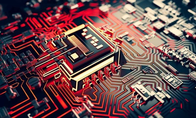
A PCB (Printed Circuit Board) is a foundational component of electronic devices, serving as a platform for interconnecting various electronic components. It’s a three-dimensional puzzle that houses intricate pathways, components, and layers. The evolution of electronics has rendered PCBs as essential elements in countless applications, from consumer electronics to industrial machinery.
Reverse engineering PCBs holds the key to understanding the designs of the past, unlocking a treasure trove of knowledge that can be harnessed for contemporary innovations. By dissecting and analyzing existing PCBs, engineers gain insights into the decisions made by their predecessors. This understanding is a launchpad for designing more efficient, compact, and high-performance circuits.
In this blog post, we embark on a journey to explore the best methods for reverse engineering PCBs. We’ll delve into the processes, techniques, and considerations that engineers must navigate to decode PCBs’ underlying structure and functionality. We’ll cover each step of this intricate process, from initial preparations to advanced software tools, from schematic reconstruction to testing and verification. Our aim is to equip engineers, hobbyists, and learners with a comprehensive guide that demystifies the art of reverse engineering PCBs.
Understanding Reverse Engineering
Reverse engineering is the process of deconstructing an object to understand its design, functionality, and components. In the realm of electronics, reverse engineering involves dissecting a PCB to comprehend its circuit PCB’s circuitry, connections, and layout. This practice is akin to unraveling a complex puzzle, with each component and trace offering clues to the larger picture.
The motivations behind reverse engineering PCBs are diverse and compelling. Engineers may engage in this practice to recreate a design that lacks documentation, to enhance or modify an existing design for a specific application, or to gain insights for educational purposes. Additionally, reverse engineering becomes crucial when dealing with legacy systems, where original documentation might be lost or incomplete.
While reverse engineering is a powerful tool, navigating legal and ethical boundaries is essential. Intellectual property rights, patents, and proprietary designs must be respected. Engaging in reverse engineering should be conducted ethically and within the confines of applicable laws. Proper authorization should be sought when reverse engineering proprietary designs or components, ensuring that ethical practices are upheld.
Initial Preparations
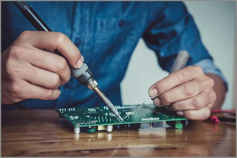
Before embarking on the journey of reverse engineering, engineers must equip themselves with a toolkit suited for the task. Tools such as magnifying glasses, multimeters, soldering irons, and oscilloscopes are essential companions on this voyage of exploration. Magnifying glasses enable close examination of small components and traces, revealing intricate details that might otherwise go unnoticed. Multimeters are invaluable for measuring voltages, currents, and resistances, aiding in the identification of component properties. Soldering irons and hot air rework stations are essential for component removal, a crucial step in invasive reverse engineering techniques.
Securing the original PCB is a crucial step in the reverse engineering process. Whether it’s salvaged from a discarded device or sourced through legitimate channels, the original PCB serves as the foundation for the entire endeavor. It physically represents the layer PCB’s circuit design, component placements, and interconnections. The original PCB is a blueprint that guides engineers in their exploration of the circuit’s inner workings.
Thorough documentation is the cornerstone of successful reverse engineering. High-resolution photographs, notes, and sketches capture the initial state of the PCB. These records serve as references during reconstruction, allowing engineers to compare their progress with the original design. Detailed photographs help capture component orientations, solder joints, and trace pathways. Notes and sketches provide additional insights into the spatial relationships between components and the overall layout.
Visual Inspection
The visual inspection phase is a critical starting point in reverse engineering. Engineers begin by meticulously examining the PCB layout and its components. This involves studying the arrangement of traces, pads, vias, and components to gain insights into the design’s structure. A closer look at the layout reveals patterns of connectivity, providing clues about the circuit PCB’s functionality.
Component markings and labels offer a wealth of information about their specifications and roles within the electronics PCB. Manufacturers often imprint part numbers, values, and polarity indicators on components. Decoding these markings is akin to deciphering the code of the PCB’s DNA. Engineers use datasheets, online resources, and industry knowledge to decode markings and understand the properties of each component.
Beyond electrical connections, the physical characteristics of components hold valuable insights. Size, shape, and placement patterns contribute to the puzzle of understanding the pcb layouting circuit’s behavior. Engineers carefully measure component dimensions and note any peculiarities that might impact their roles within the circuit. For instance, larger components might serve as heat sinks, dissipating excess heat to ensure stable operation.
Non-Invasive Techniques
Many modern PCBs feature multiple layers, each containing intricate traces and components. X-ray inspection is a non-invasive technique that allows engineers to peer through the layers, revealing hidden pathways and connections. This method is particularly useful for deciphering multi-layer PCBs, where conventional visual inspection falls short. X-ray images provide a cross-sectional view of the PCB, exposing internal structures and aiding in the identification of complex interconnections.
Thermal imaging is a powerful tool for assessing heat distribution across a PCB during operation. In electronics, excessive heat can lead to component failure and reduced reliability. Thermal cameras capture infrared radiation emitted by components, creating a thermal map of the PCB’s surface. Hotspots and temperature variations become visible, helping engineers identify areas that require attention. This technique aids in optimizing component placement and the design of heat dissipation solutions.
Invasive Techniques

De-soldering components is a delicate yet crucial process in invasive reverse engineering. Precision tools such as hot air rework stations and soldering irons are employed to carefully detach components from the PCB without causing damage. De-soldering allows engineers to access individual components for closer inspection, analysis, and potential replacement. It requires a steady hand, knowledge of soldering techniques, and an understanding of the components’ mechanical and thermal characteristics.
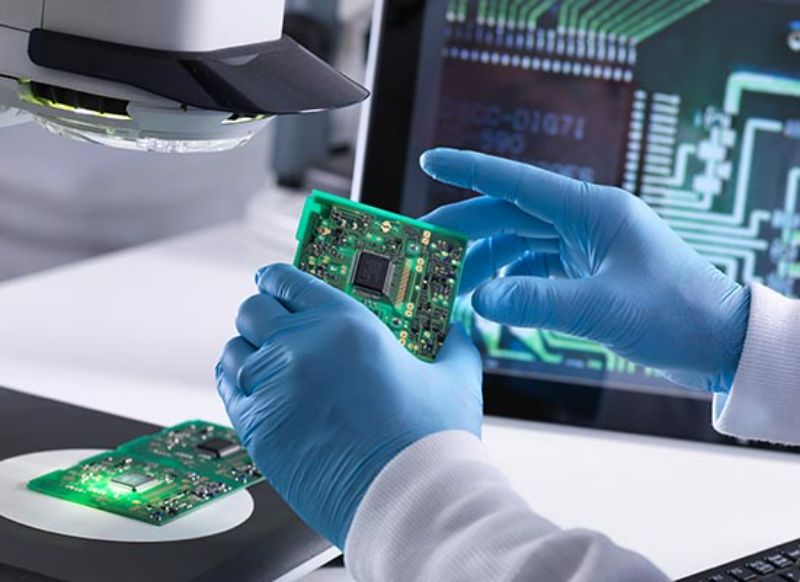
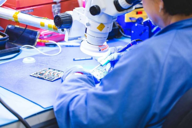
Microscopic analysis takes the exploration to a microscopic level, revealing intricate details of component structures. High-powered microscopes equipped with magnification capabilities enable engineers to examine components at a level of detail that is impossible with the naked eye. This analysis unveils the construction of integrated circuits (ICs), surface-mounted devices (SMDs), and discrete components. Engineers can identify wire bonds, die sizes, packaging methods, and other features that contribute to component functionality and performance.
Circuit tracing is a fundamental technique for reverse engineering PCBs. It involves systematically tracing the pathways of electrical signals across the PCB to reconstruct the schematic diagram. By identifying connections, junctions, and nodes, engineers gradually piece together the pcb layouting circuit’s logical structure. Advanced multimeters with continuity testing capabilities and specialized probing tools aid in this process. As traces are traced, engineers visually represent the circuit’s connectivity, paving the way for schematic reconstruction.
Component Identification
Decoding integrated circuit (IC) part numbers is a critical step in reverse engineering. Integrated circuits house complex circuitry within a compact package. Deciphering IC part numbers provides vital information about the IC’s manufacturer, series, specifications, and functionalities. Datasheets and online databases are pivotal in deciphering these part numbers, helping engineers select appropriate replacements or equivalents during reconstruction.
Identifying passive and active components is crucial for understanding the pcb layouting circuit’s behavior. Passive components, such as resistors, capacitors, and inductors, do not amplify signals. Active components, such as transistors and integrated circuits, amplify or manipulate signals. Recognizing these distinctions aids in comprehending the circuit’s interactions and behavior. Engineers identify passive and active components based on their characteristics, packaging, and roles within the circuit.
Researching and sourcing components is a continuous endeavor during reverse engineering. The availability of exact replacements or equivalents contributes to the accuracy and functionality of the reconstructed design. Engineers turn to electronic component distributors, online marketplaces, and datasheets to identify suitable replacements. Collaboration within engineering communities can provide insights into sourcing strategies and compatible alternatives when dealing with legacy components or proprietary parts.
Schematic Reconstruction
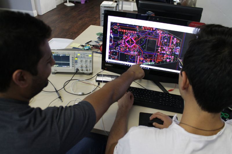
Creating a preliminary schematic diagram is a pivotal step in reverse engineering. Engineers use specialized software tools to translate the information gathered during the earlier stages into a digital representation. This diagram captures component placements, connections, and signal flow. The preliminary schematic serves as a visual guide for further analysis and validation.
Validating the schematic’s accuracy through analysis is a meticulous process. Engineers compare the schematic’s logical connections and pathways with the physical components and traces on the original PCB. Any discrepancies or inconsistencies are carefully examined, and adjustments are made to ensure an accurate representation. This iterative process involves refining the schematic, revisiting the physical PCB, and verifying the correspondence between the two.
Reverse Engineering Software Tools
PCB design software plays a pivotal role in the reverse engineering process. Engineers use these tools for schematic capture, translating the preliminary schematic into a digital format. Components are placed, connected, and annotated within the software, creating a digital blueprint of the reconstructed design. This digital representation offers flexibility, easy sharing, and the potential for further design modifications.
PCB layout tools are used to recreate the physical layout of the PCB based on the digital schematic. Components are placed in designated locations, traces are routed to establish connections, and design rules are followed to ensure manufacturability. PCB layout tools offer features such as autorouting, design rule checks, and three-dimensional visualization, ensuring that the reconstructed layout aligns with the original design’s specifications.
Circuit simulation tools are employed to validate the reconstructed schematic’s behavior before physical implementation. These tools enable engineers to simulate the circuit’s performance under various conditions, input signals, and component tolerances. By simulating the circuit’s response, engineers can identify potential issues, refine the design, and predict its behavior. Circuit simulation enhances confidence in the accuracy and functionality of the reverse-engineered design.
Testing and Verification
The assembled reverse-engineered PCB undergoes functional testing to validate its behavior. Input signals are applied, and the PCB’s responses are compared against the expected results derived from the reconstructed schematic. Functional testing helps identify discrepancies, errors, or deviations from the original design’s behavior.
During functional testing, any discrepancies or errors are thoroughly examined. This stage is a critical quality check to ensure that the reverse-engineered PCB faithfully represents the original design. Engineers meticulously compare input-output relationships, signal responses, and circuit behaviors to identify inconsistencies and diagnose potential problems.
Challenges and Solutions
Reverse engineering electronics PCBs present engineers with various challenges that demand creative solutions. One common challenge is tackling complex multi-layer PCBs. These designs contain multiple stacked layers, each hosting intricate traces and components. Navigating these dense designs requires specialized tools, such as high-resolution X-ray systems that can penetrate layers and reveal connections. Engineers employ layer-by-layer analysis to unveil the hidden pathways, ensuring a comprehensive understanding of the PCB’s architecture.
Another challenge arises when dealing with components that possess obscured markings or labels. Some components might lack visible part numbers or bear markings that have faded over time. Engineers resort to alternative techniques such as component measurement, circuit tracing, and cross-referencing with datasheets in such cases. The ability to decode components without relying solely on markings showcases the resourcefulness and expertise of engineers engaged in reverse engineering.
Custom and proprietary components pose unique challenges due to their specialized nature. Manufacturers might use custom components to differentiate their products or enhance performance. When reverse engineering such components, engineers rely on a combination of techniques. Comparative analysis with known components, circuit tracing, and functional testing play a crucial role in deciphering the properties and roles of these components. Collaboration within the engineering community can also offer valuable insights and strategies for dealing with proprietary components.
Practical Applications
The art of reverse engineering PCBs extends beyond curiosity and exploration. It finds practical applications across various domains. One notable application is utilizing reverse engineering for legacy PCBs. In cases where documentation is unavailable or outdated, reverse engineering becomes a vital tool for understanding and preserving the functionality of legacy systems. Engineers can recreate or adapt these designs to meet modern standards and requirements.
Adapting existing designs for new applications is another avenue where reverse engineering shines. When a proven design meets new challenges, reverse engineering offers a head start in redesigning the circuit for a different purpose. Whether it’s repurposing a circuit for a different industry or incorporating modern components, the insights gained from reverse engineering streamline the adaptation process.
Reverse engineering also plays a significant role in education. Students and learners benefit from dissecting and reconstructing existing PCBs, gaining hands-on experience in circuit analysis, schematic reconstruction, and design principles. This practice cultivates a deeper understanding of electronics and encourages critical thinking in the realm of circuitry.
Ethical Considerations
While reverse engineering is powerful, it must be wielded ethically and responsibly. Respecting intellectual property rights is of utmost importance. Designs protected by patents, copyrights, and trade secrets deserve acknowledgment and adherence to legal boundaries. Proper authorization should be sought when reverse engineering proprietary designs, and the rightful intellectual property owners should be recognized.
Proper attribution is a cornerstone of ethical reverse engineering. Engineers who unveil insights through reverse engineering should acknowledge the original designers and their contributions. This demonstrates professionalism and fosters a culture of collaboration and respect within the engineering community.
Balancing reverse engineering with innovation is a delicate task. While reverse engineering provides valuable insights, innovation involves creating new solutions. Engineers should strive to leverage the knowledge gained from reverse engineering to drive innovation forward, enhancing existing designs and pioneering novel approaches.
Conclusion
The journey through the intricate landscape of reverse engineering PCBs unveils a realm where curiosity meets innovation. From initial preparations to non-invasive and invasive techniques, from component identification to schematic reconstruction, engineers traverse a path that unlocks the mysteries of existing designs.
Reverse engineering is not merely an exploration of the past; it’s a catalyst for future advancements. As engineers decode the secrets of PCBs, they equip themselves with the knowledge to innovate, adapt, and build upon the foundations laid by their predecessors. By embracing ethical practices, respecting intellectual property rights, and balancing reverse engineering with creativity, engineers shape a future where the boundaries of possibility are continually expanded.
In this guide, we’ve delved into the essence of reverse engineering PCBs. We’ve explored techniques that dissect intricate designs, uncovering pathways of connectivity and unraveling the logic woven into each trace. As the circuits come to life under the watchful eyes of engineers, the journey of reverse engineering becomes a testament to human ingenuity and the unquenchable thirst for understanding.
As you embark on your own journey of reverse engineering, may this guide serve as a beacon of knowledge, guiding your steps as you navigate the complexities of PCBs and draw inspiration from past designs. The world of reverse engineering awaits, ready to reveal its secrets to those who dare to venture forth.
This article is so useful, I’ve been learning a lot from it. Thank you