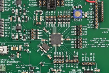
Most common boards are built on 4-layer PCB design as long as they do not have very high power requirements, high speed requirements on multiple layers, or high I/O count. Once one of these functional requirements emerges in a design, or when component densities get very high, it’s time to increase the layer count and possibly use a 6-layer PCB stack-up. These devices will take you into the next level of complexity, and yet they are actually preferable to a 4-layer board in terms of routability, power integrity, signal integrity, and EMC.
The best way to ensure your 6-layer PCB will operate correctly is to start with a stack-up and to get it qualified with your manufacturer. Different 6-layer PCB stack-ups are ideal for different applications, and the PCB stack-up will be the biggest determinant of EMC and routing ability. However, there are some simple guidelines that can be followed to help ensure SI, PI, and EMC in your system.
Starting a 6-Layer PCB Design
The main reason we use a 6-layer design is to get access to additional power, additional signal, or both. I’ll show an example 6-layer PCB stack-up below, which supports many advanced products that do not require extremely high IO count. The normal set of PCB routing guidelines applies in a 6-layer PCB, but one important point to consider is how to route power in the design. I’ll discuss this below as well.
6-Layer PCB stack-up
An example PCB stack-up for a 6-layer circuit board is shown below. This example places a signal layer and a power layer in the internal layers of the PCB. The idea here is to transition away from the Sig+GND/PWR/Sig/GND+Sig arrangement that would be typical in a 4-layer PCB when higher component density and more routing channels are needed. The addition of the power plane in the internal layer also provides strong decoupling for power integrity, and it allows the devices to provide more power than might be available in a 4-layer PCB Design.

This PCB Design stack-up can use thinner outer dielectrics to support impedance control on the surface layer for high speed signals or RF routing. It is usually the best idea to always have GND planes placed on L2 and L5 to provide shielding for the inner signal layer and decoupling for the power-ground plane pair on L2-L3. This also shields L4 and L6 to suppress crosstalk.
Aside from these points with the stack-up design, the standard set of high speed PCB routing guidelines should be followed in these boards. If you’re using a high pin count BGA in the PCB layout, these devices can be challenging as they will require multiple vias passing through the stack-up in order to make connections to the internal power layer and the surface layers. The result is that there is a risk that the GND planes get cut up too much and will not provide enough capacitive coupling for the signal return path.
Should this happen, it is then appropriate to use grounded copper pour on the external layer to provide the required grounding for digital signals. This has the additional benefit of shielding for any RF sections on the board as long as properly spaced stitching vias are used in the layout. Make sure to consider these points at the end of the routing phase during a PCB design review.
Power Planes and Rails
Although the above 6-layer PCB stack-up example dedicates a single layer to power rails to support high current nets, it’s still appropriate to put a rail on a signal layer. You should be careful with this; if you’re routing the power rail on L4 with L3 dedicated to an entire power layer, the two rails can couple to each other capacitively, which can create a source of EMI at high frequencies when both rails switch. However, if there is ground on the surrounding layers (L2 and L5), this will balance the capacitive coupling to GND as you now effectively have a Pi filter built from capacitors. The coupling to the GND planes will be much more effective in directing a displacement current than the potential difference between the two rails, so these planes will dominate the electromagnetic excitation that arises in the PCB stack-up.

Applications of 6-Layer PCBs
If you’re unsure whether you need a 6-layer PCB Design instead of a 4-layer or 8-layer PCB, it always helps to look at some application examples of these boards. The entire goal of a 6-layer board is to provide additional power or signal that would normally be lacking in a 4-layer board so that your product can have more advanced capabilities. Some of the ideal application areas for a 6-layer PCB include:
- Devices supporting multiple high speed interfaces. For example, our data center and networking equipment designs are built on 6-layer boards. These products support multiple multi-Gbps Ethernet channels in an aggressive form factor.
- mmWave PCBs, such as radar modules; the top layer can be a low-loss PTFE laminate to provide routing for RF signals. We’ve built multiple radar modules that implement LVDS, CSI, Ethernet, and/or PCIe on 6-layer boards.
- Devices requiring high power and high speed digital/high frequency analog in the same board. High power can be implemented using two power planes on the internal layers with GND on L2 and L5.
- Designs with high component density on a single layer, including high speed components. The power plane can easily provide power directly to the component layer, and there will be two dedicated signal layers with ground to support low speed signals and controlled impedance.
- Mixed-signal PCB design with a dedicated analog section (bottom layer) and high digital component density on the top and internal layers, including high speed digital interfaces.
- Devices with multiple moderate ball count BGAs and low IO count. Once ball counts and IO counts get very large with fine pitch, a higher layer count will be needed to route everything in the design.
From the above list, it should be clear that a 6-layer board will be the first departure most designers will make from a standard 4-layer board in advanced systems. As the number of digital interfaces in the design scales higher and footprint scales smaller, the required layer count will increase further. If you’re unsure where to start and what PCB Design stack to use in your PCB Design, make sure you contract with a design firm that understands how to design and manufacture these boards to the highest quality and reliability specifications.

When you’re ready to start your next 6-layer PCB Design, you should work with a design firm that understands how to build and qualify these PCB stack-ups for EMC, noise, power integrity, and manufacturability. PCBLOOP helps consumer OEMs, industrial primes, commercial space companies, and electronic equipment companies in multiple industries design modern PCBs and create cutting-edge embedded technology. We’ve also partnered directly with EDA companies and ITAR-compliant PCB manufacturers, and we’ll make sure your next design is fully manufacturable at scale. Contact PCBLOOP for a consultation.
