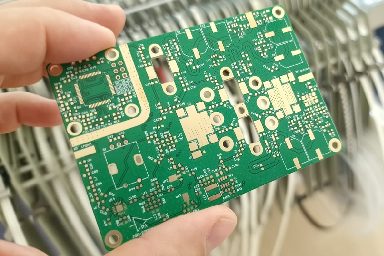
During PCB fabrication, exposed conductors on surface layers are coated with copper and copper oxidizes that degrade if left exposed. Therefore, PCB plating on the surface layers is completed with an intermetallic surface finish. The surface finish provides a solderable surface for components and a durable protective surface. There are several PCB surface plating materials to choose from. Let’s take a look at the most common options that are compatible with the standard PCB manufacturing process.

Standard PCB Surface Platings
Immersion Tin (ImSn)
A chemical process is used to deposit a thin layer of tin on the copper finish up to the required plating thickness. This type of plating is particularly suitable for high-speed circuits and it is a good option for fine pitch components with flat surface requirements. However, diffusion may occur between overlapping copper and tin layers. ImSn is also known to experience a problem of tin ‘whisker’ growth in certain environmental conditions or operating conditions.
Immersion Silver (ImAg)
This PCB surface coating is similar to ImSn and is usually utilized in nickel-free PCBs with that support high-speed digital applications. It’s a great choice for EMI shielding, dome contacts, and wire bonding. ImAg is a non-electrolytic chemical finish that is a better choice for higher frequency/speed applications than HASL and ENIG. Immersion silver is also preferable in high-frequency PCB design as it does not create additional roughness losses on bare copper, but it comes with higher costs.

Hot Air Solder Levelling (HASL)/Lead-free HASL
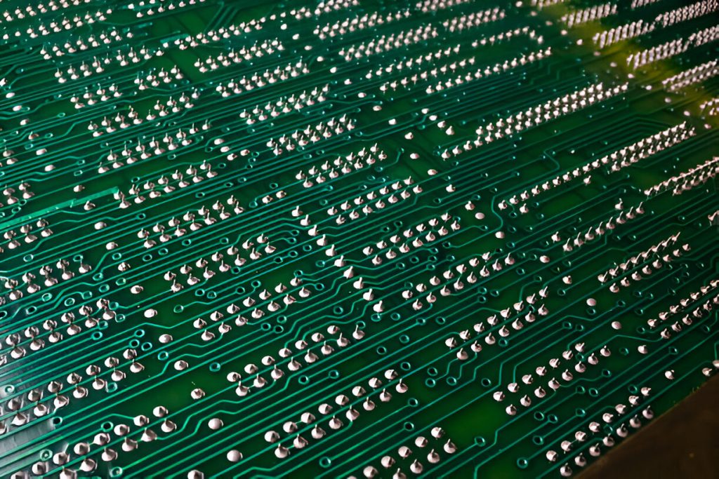
HASL is one of the standard PCB surface plating options used in the industry. The deposition procedure involves immersing the PCBs in a vat of molten solder, i.e., tin/lead alloy, followed by eliminating extra solder with ‘air knives’. This means that hot air is blown across the board’s surface to get rid of the extra solder. The PCB is held by vertical clamps to ensure the plated layer has a homogeneous thickness. Currently, mil-aero circuit boards top the list of frequent HASL users. HASL surface finish can also be done without lead (lead-free HASL), which is a great option for entry-level plating. Furthermore, HASL plating provides an early warning of any potential delamination difficulties before assembly because the procedure exposes the board to temperatures of up to 265 °C.

Electroless Nickel Immersion Gold (ENIG)
This finish adds a thin, solderable gold layer on top of copper traces. This plating technology requires a nickel barrier between the gold layer and the copper traces to provide adhesion. The general thickness range of the gold layer is 2-8 micro-inches and the nickel layer is 120-240 micro-inches. The nickel layer also forms a barrier to protect the copper from oxidation and it is the real surface on which the electronic components are soldered. The gold provides low contact resistance and shields the nickel during storage. ENIG is a great plating option that provides a long-lasting, durable alternative to lead-based materials.

Electroless Nickel Electroless Palladium Immersion Gold (ENEPIG):
As the name implies, this is a triple metallic finish with layers of nickel, palladium, and gold. This is perhaps the best option for printed circuit boards that need wire bonding. As in the case of ENIG, a layer of nickel is coated on top of the bare copper to provide adhesion. After that, to prevent nickel oxidation and copper diffusion, a palladium protective layer is applied. The final gold layer provides an additional barrier against degradation and oxidation.

Hard Gold
In ENIG and ENEPIG, the layer of gold is very thin and susceptible to degradation due to mechanical damage and scratches. To counter this problem, a layer of hard gold is applied on top of the nickel for a finish that is both durable and resistant to corrosion. This form of PCB surface plating is utilized in applications that require frequent mechanical contact, such as buttons and keypads because it is very durable. Hard gold’s high cost and low solderability make it more difficult to solder.

Organic Solderability Preservative (OSP)
This surface finish protects the copper layer from oxidation through deposition of a very thin layer of an organic water-based protective substance. This is typically applied in a conveyorized process. In contrast to other PCB surface plating materials, organic compounds are more susceptible to handling and contamination. They also have a shorter shelf life. However, they do not increase the roughness losses of the copper foil in the PCB, making this plating comparable to ImAg for high-frequency applications.

Carbon Ink
This type of PCB surface finish involves covering copper on the PCB with a layer of carbon-based conductive ink for protection. Controlling the printing process, baking time and temperature, and the resistance of the film is crucial to manufacturing carbon ink PCBs. Screen printing can be used to print carbon ink onto PCBs. Carbon ink surface plating is an economical choice because of its simple plating procedure and the low cost of the ink.

PCB Plating Thickness
Surface finish selection is the most significant phase in PCB fabrication since it affects yields, field failure rate, performance, shelf-life, test capabilities, and costs. In addition to the surface finish material, the thickness of the PCB surface plating layer is important to achieve the desired functionality of the PCB. For instance, plating thickness and material are at mmWaves frequencies due to the need for low roughness; immersion silver is preferred for this application area.
You can probably get away with ignoring the thickness in the case of low frequencies and low-speed digital signals, but at higher frequencies like in short-range radar applications, PCB plating thickness has a significant effect on losses. Moreover, IPC standard compliant designs need to follow the specified minimum plating thickness defined in either the IPC-2221A standard, or the IPC-601x family of standards.
At PCBLOOP, we regularly work with high speed PCB design and RF systems that require careful consideration of PCB surface plating materials. We know how to create a high quality, fully manufacturable PCB layout for your system. We’re here to help electronics companies design modern PCBs and create cutting-edge technology. We’ve also partnered directly with EDA companies and advanced PCB manufacturers, and we’ll make sure your next layout is fully manufacturable at scale. Contact PCBLOOP for a consultation.
Greetings! Very helpful advice in this particular article! It is the little changes that will make the largest changes. Many thanks for sharing!