Hello everyone, and welcome to our post on PCB Design 101: Everything You Need to Know. If you’re new to the world of PCB design or just looking to brush up on your skills, you’ve come to the right place.
What is a PCB?
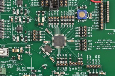
First things first, let’s talk about what a PCB actually is. A PCB, or printed circuit board, is a board made of insulating material with conductive pathways etched onto its surface. These pathways connect electronic components, allowing them to work together and create a functioning electronic device. PCBs can come in a variety of shapes and sizes, depending on the intended use of the device they will be a part of.
The PCB Design Process
Now that we know what a PCB is, let’s dive into the PCB design process. The first step is to create a schematic diagram of your circuit, which shows how all the components are connected. This is typically done using software tools such as Eagle, Altium, KiCad or Allegro. Once you have your schematic in place, it’s time to move on to laying out the PCB itself.
During the PCB layout process, you’ll need to decide where each component will go and how the conductive pathways will be routed. This can be a complex and time-consuming process, as you need to ensure that everything is laid out in a way that makes sense for the device’s intended use and doesn’t create any unnecessary challenges during manufacturing.
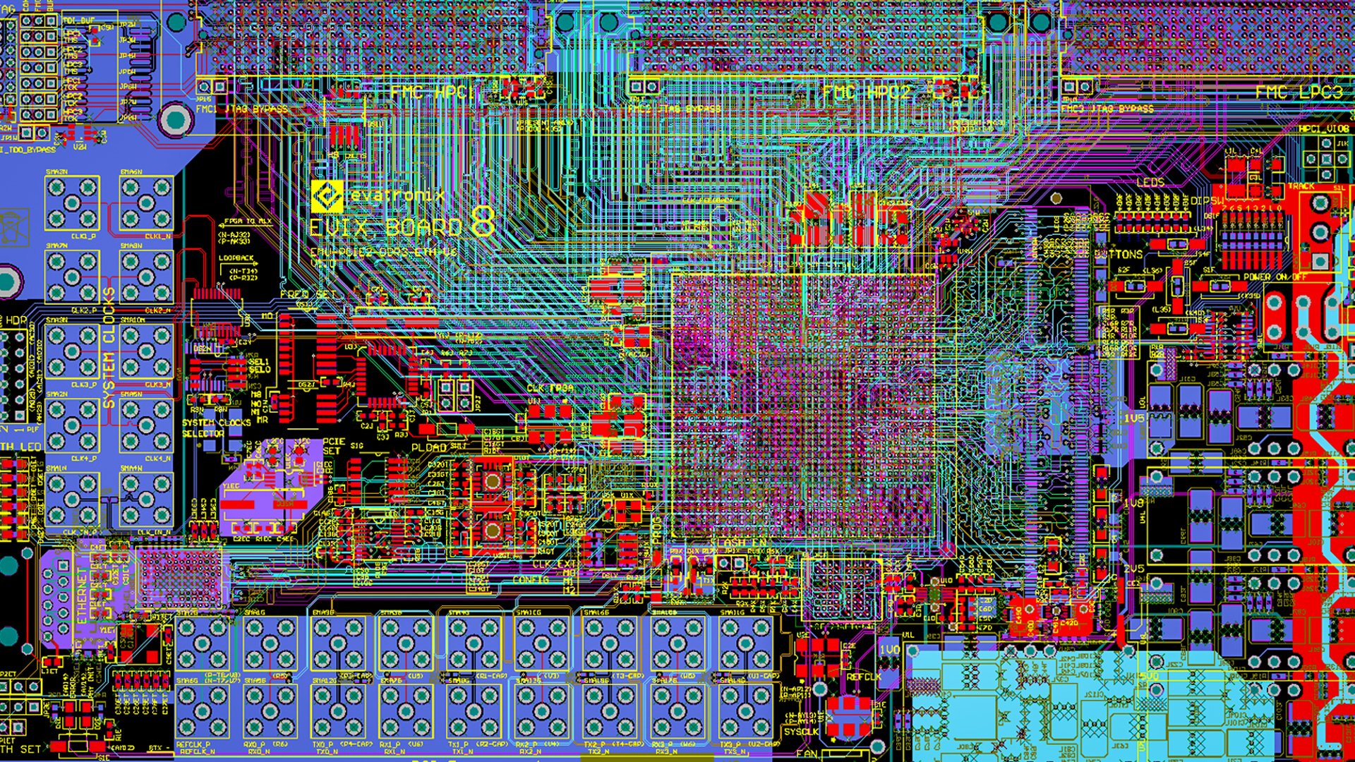
Once you have a layout in place, it’s time to generate Gerber files, which are used by manufacturers to produce your PCB. These files provide detailed instructions for how to etch the conductive pathways onto the PCB, as well as how to drill any necessary holes.
Key Considerations in PCB Design
here are several key considerations you need to keep in mind during the PCB design process. These include:
Component placement: You want to make sure all the components are laid out in a way that makes sense for the device’s intended use and doesn’t create any unnecessary challenges during manufacturing. It’s also important to keep in mind any potential sources of interference, such as noisy components or high-voltage traces.
Trace width and spacing: These parameters need to be chosen based on the amount of current the traces will be carrying and the voltage they’ll be carrying. You’ll also need to take into account any potential sources of noise, such as electromagnetic interference (EMI).
Power and ground planes: These planes are used to provide stable and low-impedance power and ground connections throughout the PCB. They can be especially important in high-speed designs, where even small amounts of noise can cause problems.
Signal integrity: You’ll want to ensure that signals don’t degrade or interfere with each other as they travel through the PCB. This can be achieved through careful placement of components and routing of traces, as well as the use of techniques such as differential signaling.
Thermal considerations: Depending on the power dissipation of your components, you may need to take steps to ensure that your PCB doesn’t overheat. This can include adding heat sinks or thermal vias to conduct heat away from the components.
PCB Design Tools
Now that we’ve covered the design process and key considerations, let’s talk about the tools you’ll need to design your own PCB. There are several software tools available, ranging from free to expensive. We’ll go over some of the most popular options and what sets them apart.
In order to design a PCB, you will need to use specialized software that enables you to create the schematic, lay out the components, and generate the Gerber files that are needed to manufacture the board. There are a variety of different PCB design tools available, ranging from free open-source software to professional-level applications that can cost thousands of dollars.
Some of the most popular PCB design tools on the market today include Altium Designer, Eagle PCB, KiCAD, OrCAD, PADS, and Allegro. Each of these tools has its own unique set of features and capabilities, so it’s important to do your research to determine which one will best meet your needs.
One of the key considerations when selecting a PCB design tool is the ease of use. Some tools are more intuitive and user-friendly than others, which can be a major factor if you’re new to PCB design. Additionally, you’ll want to look for a tool that offers a robust set of features and the ability to create complex designs with multiple layers.
Another consideration is the cost of the tool. Some of the more advanced PCB design tools can be quite expensive, which may not be feasible for smaller businesses or individuals. However, there are also many free or low-cost options available, which can be a good starting point for those who are just getting started with PCB design.
Regardless of which tool you choose, it’s important to take the time to learn how to use it properly. Most PCB design tools offer extensive documentation, tutorials, and support resources to help you get started, and there are also many online communities and forums where you can connect with other designers to ask questions and get advice.
In conclusion, PCB design is a complex and challenging field that requires a combination of technical knowledge, creativity, and attention to detail. Whether you’re a professional engineer, a hobbyist, or a student, there are many resources available to help you learn and master the art of PCB design. With the right tools, techniques, and a bit of practice, you can create high-quality, reliable PCBs that meet the needs of a wide range of applications. So why not give it a try and see what you can create?