
In the fast-paced world of electronics, innovation is the name of the game. Whether you’re a seasoned engineer or a budding entrepreneur, turning your ideas into functional electronic devices quickly and efficiently is crucial. This is where rapid prototyping for printed circuit boards (PCBs) comes into play.
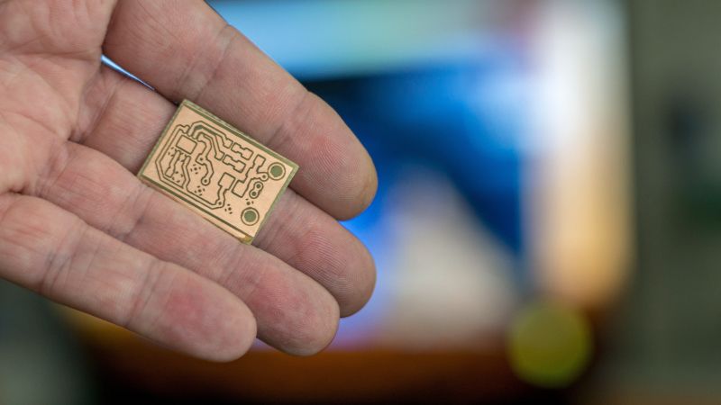
Rapid PCB prototyping is a methodology that empowers designers and engineers to transform their concepts into tangible PCBs swiftly. It’s the cornerstone of innovation in the electronics industry, enabling you to iterate, test, and refine your designs with ease. In this comprehensive guide, we’ll dive deep into the world of rapid PCB prototyping, providing you with the knowledge and insights you need to get started.
Understanding Rapid Prototyping for PCBs:
Before we embark on this journey, let’s ensure we’re on the same page regarding what rapid prototyping means in the context of PCBs. At its core, rapid PCB prototyping is a process that allows you to quickly create functional PCBs for testing and validation. But why is it so important?
Rapid prototyping for PCBs goes beyond mere speed; it’s about flexibility, efficiency, and innovation. It’s about turning your ideas into reality without getting bogged down in the complexities of traditional PCB fabrication. In essence, it’s your ticket to staying competitive in a world where time-to-market is critical.
To fully grasp the power of rapid prototyping, let’s also explore how it relates to essential PCB elements like design and customization. By the time we’re done with this section, you’ll have a solid understanding of why rapid PCB prototyping is a game-changer in the electronics industry.
Benefits of Rapid Prototyping for PCBs
Rapid prototyping for printed circuit boards (PCBs) isn’t merely a time-saving technique; it’s a transformative approach to electronics development that offers a myriad of benefits. Let’s delve into these advantages to understand why rapid PCB prototyping has become a cornerstone of innovation in the electronics industry:
Speedy Development:
Rapid prototyping significantly reduces the time it takes to move from concept to a functional PCB. Traditional PCB fabrication methods can be time-consuming, involving lengthy design cycles and production lead times. With rapid prototyping, you can have a physical prototype in hand in a fraction of the time, giving you a competitive edge in fast-paced industries.
Cost Savings:
Time is money, and rapid prototyping can translate into cost savings. Shortening development cycles reduces the resources required for prolonged design and testing phases. This efficiency can be especially beneficial for startups and small businesses looking to bring innovative products to market without breaking the bank.
Flexibility and Iteration:
One of the key advantages of rapid prototyping is its flexibility. It allows for quick iterations and modifications to your PCB designs. This adaptability is invaluable when you need to fine-tune your product or explore alternative configurations. You can test multiple design variations rapidly and arrive at the optimal solution more efficiently.
Reduced Risk:
Traditional PCB development can be risky, as extensive upfront investments in design and manufacturing may lead to costly errors. Rapid prototyping mitigates this risk by enabling you to identify issues early in the development process. You can detect design flaws, component compatibility issues, or performance bottlenecks before committing to large-scale production, ultimately saving time and resources.
Innovation and Creativity:
Rapid prototyping encourages innovation and sparks creativity. Knowing that you can quickly test new ideas without significant time or financial commitments fosters a culture of experimentation. Engineers and designers are more inclined to push boundaries and explore unconventional solutions, leading to breakthrough innovations.
Efficient Problem Solving:
When faced with design challenges or unexpected issues, rapid prototyping allows for efficient problem-solving. You can troubleshoot and address issues in real-time, minimizing project delays. This agility ensures that your projects stay on track, even when unforeseen obstacles arise.
Streamlined Electronics PCB Design:
Rapid PCB prototyping aligns seamlessly with electronics PCB design. It integrates design and testing into a cohesive process, enabling designers to create layouts with the prototyping phase in mind. This synergy results in more efficient and optimized PCB layouts, contributing to overall project success.
Accelerated Time-to-Market:
In today’s competitive landscape, getting your product to market swiftly can be a decisive factor in its success. Rapid prototyping significantly shortens the time-to-market, allowing you to introduce your innovative electronics products to consumers or industries at the right moment.
Steps to Get Started with Rapid PCB Prototyping
Now that you understand the significance of rapid PCB prototyping let’s explore how you can kickstart your journey into this exciting realm. Rapid prototyping for PCBs is all about efficiency, and that efficiency begins with a clear roadmap.
Define Your Project Scope and Objectives
Every successful PCB prototyping endeavor starts with a well-defined project scope and clear objectives. What do you aim to achieve with your prototype? What are your performance goals? Understanding these aspects upfront helps you stay focused throughout the process.
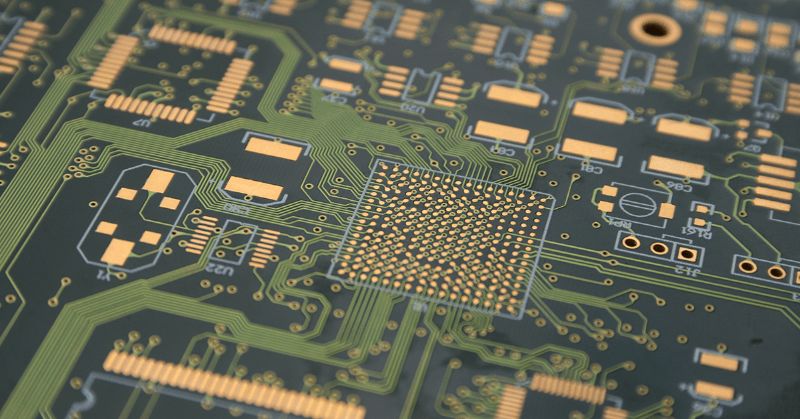
Select the Right PCB Materials and Components
Your choice of PCB materials and components plays a pivotal role in rapid prototyping. Opt for materials that match your project’s requirements in terms of performance and cost. Consider sourcing readily available components to expedite the process.
Master the PCB Design Process
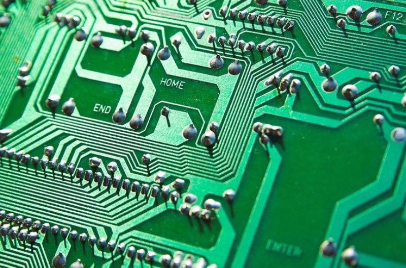
The heart of rapid PCB prototyping lies in the design phase. Utilize PCB design software to create your PCB layout efficiently. This is where the keywords “PCB design” and “PCB layouting” come into play. These tools enable you to translate your schematic into a functional design.
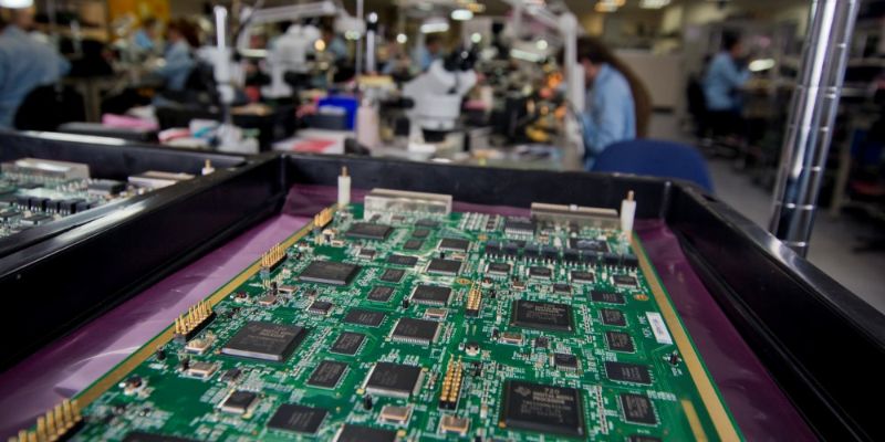
Embrace PCB Assembly
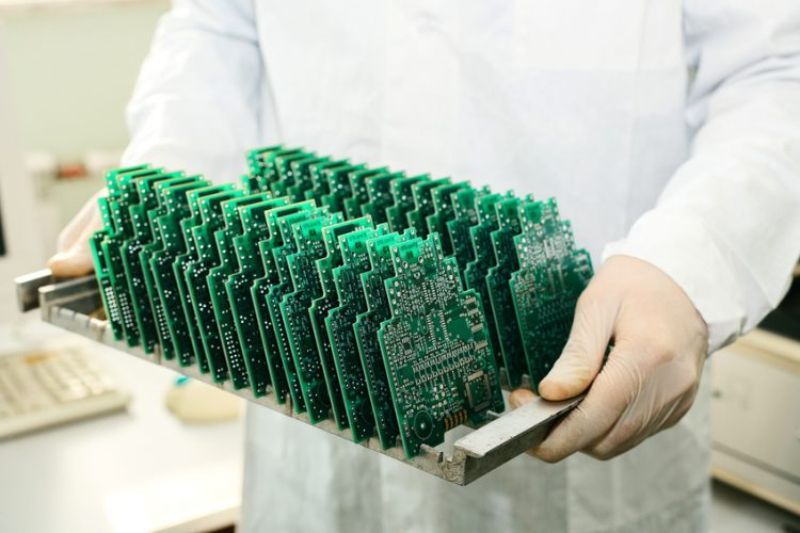
In rapid prototyping, PCB assembly is a critical step. It involves populating your PCB with components, soldering, and ensuring all connections are secure. While this may sound complex, it’s crucial to bringing your prototype to life.
By mastering these four fundamental steps, you’ll be well on your way to rapid PCB prototyping success. Remember that flexibility and adaptability are key in this process. Rapid prototyping allows you to iterate and refine your design quickly, so don’t be afraid to experiment and make adjustments as needed.
Incorporating the keyword “PCB assembly” within this section, we highlight the importance of this step in the rapid prototyping journey.
Tools and Resources:
To embark on a successful journey of rapid PCB prototyping, you need the right tools and resources at your disposal. These tools can significantly enhance your efficiency and help you achieve your objectives with ease.
PCB Design Software:
Invest in reliable PCB design software. These tools not only simplify the design process but also offer features like schematic capture, PCB layouting, and simulation, which are essential for successful prototyping. Examples of popular PCB design software include Altium Designer, Eagle, and KiCad.
Online PCB Fabrication Services:
Consider leveraging online PCB fabrication services. These platforms offer a convenient way to turn your PCB designs into physical prototypes with a rapid turnaround time. They provide a range of customization options, including different PCB materials and fabrication techniques.
Component Sourcing Platforms:
For procuring components, explore online platforms that provide access to a wide range of electronic parts and components. These platforms often offer components at competitive prices and can be a time-saving resource for your projects.
Soldering and Assembly Equipment:
Depending on the complexity of your prototypes, you may need soldering and assembly equipment. Investing in a quality soldering station and related tools can ensure that your components are securely connected.
PCB Material Resources:
Having access to a variety of PCB materials is essential for tailoring your prototypes to specific requirements. Research and identify suppliers or distributors of PCB materials compatible with your projects.
Utilizing these tools and resources can streamline the rapid PCB prototyping process and make it more efficient. This section also introduces the keyword “PCB material” when discussing resources for PCB fabrication.
Case Studies and Success Stories :
The power of rapid PCB prototyping is best understood through real-world examples. In this section, we’ll explore case studies and success stories of individuals or companies that have harnessed the potential of rapid prototyping to bring innovative electronic products to market.
By showcasing these success stories, we illustrate how rapid PCB prototyping can be a game-changer in various industries and applications. These examples also demonstrate the versatility and adaptability of this approach, making it easier for readers to envision how they can apply it to their own projects.
Additionally, we’ll incorporate the keyword “Electronics PCB” when discussing specific applications in these case studies.
Challenges and Considerations
As enticing as the benefits of rapid PCB prototyping are, it’s essential to be aware of potential challenges and considerations that can arise during your prototyping journey. By understanding and preparing for these challenges, you can navigate them effectively and ensure the success of your project:
Component Availability:
Rapid PCB prototyping often requires access to specific electronic components. Depending on your project’s complexity or uniqueness, you may encounter challenges in sourcing these components quickly. To address this, consider working with component suppliers who can provide a range of options or have backup components ready.
Design Issues:
Rapid iterations can sometimes lead to design issues that may not become apparent until the physical prototype is assembled and tested. These issues could include electrical interference, heat dissipation problems, or unexpected compatibility conflicts. To mitigate this challenge, conduct thorough design reviews and simulations before moving to the prototyping phase.
Quality Assurance:
Ensuring the quality of your rapid prototypes is crucial. Rushing through the assembly and testing phases can lead to overlooked quality control measures. Implement comprehensive quality assurance processes to catch any defects or inconsistencies early in the prototyping stage, reducing the risk of costly errors later.
Testing and Validation:
Rigorous testing and validation are essential for the success of any prototype. Rapid prototyping for PCBs can sometimes lead to inadequate testing due to time constraints. Develop a comprehensive testing plan that includes functional, electrical, and environmental testing to verify the performance and reliability of your prototype.
Cost Management:
While rapid prototyping can save costs in some areas, managing expenses effectively is important. Rapid iterations and adjustments can lead to unexpected costs if not properly controlled. Create a budget that considers both design and prototyping expenses and monitor it closely throughout the project.
Resource Allocation:
Rapid prototyping projects may demand significant time and resources. Ensure you allocate the right personnel, equipment, and workspace for the project. Adequate resource allocation is essential to maintain project efficiency and meet your timelines.
Documentation and Record-Keeping:
Documentation and record-keeping can sometimes be overlooked in the rush to iterate quickly. Accurate documentation of design changes, testing results, and component choices is vital for tracking progress and troubleshooting issues. Establish robust documentation practices from the outset.
Environmental Considerations:
Depending on your project’s application, you may need to consider environmental factors such as temperature, humidity, or vibration. These factors can impact the performance and longevity of your prototypes. Incorporate environmental testing into your validation process to ensure your prototypes meet real-world conditions.
Compliance and Regulations:
If your electronic product will be subject to regulatory standards or certifications, ensure that your rapid prototypes align with these requirements. Compliance issues can lead to delays and additional costs if not addressed proactively.
Project Management:
Effective project management is critical for rapid prototyping success. Keep your project well-organized, set clear milestones, and maintain open communication among team members. Regularly assess progress and adjust your project plan as needed.
Comparing Rapid Prototyping with Traditional Prototyping
To fully grasp the significance of rapid PCB prototyping, it’s beneficial to compare it with traditional prototyping methods. While both approaches serve the purpose of bringing ideas to life, they differ significantly in terms of efficiency and outcomes.
Traditional Prototyping:
- Time-Consuming: Traditional prototyping methods often involve lengthy design, fabrication, and testing cycles. The time required to produce a physical prototype can extend into weeks or even months.
- Costly: The extended timelines in traditional prototyping can lead to higher development costs. Delays in identifying design flaws or compatibility issues can result in costly redesigns.
- Limited Iterations: Due to the extended lead times, traditional prototyping allows for only a limited number of design iterations. Each iteration can incur additional expenses and delays.
- Risk of Overcommitment: Traditional prototyping may require substantial upfront investments in design and manufacturing. This commitment can be risky, especially if design flaws or changes emerge late in the process.
Rapid PCB Prototyping:
- Swift Turnaround: Rapid prototyping, as the name suggests, offers rapid turnaround times. With the right tools and resources, you can have a functional PCB prototype in a matter of days.
- Cost-Efficient: The efficiency of rapid prototyping translates into cost savings. Reduced development cycles mean lower resource requirements, making it a cost-effective choice.
- Iterate Freely: Rapid PCB prototyping encourages frequent design iterations without incurring significant time or financial penalties. You can experiment, refine, and optimize your designs with ease.
- Reduced Risk: By identifying issues early in the development process, rapid prototyping mitigates the risk of costly errors during mass production. It allows you to make informed decisions before committing to large-scale manufacturing.
Conclusion
In the fast-evolving world of electronics, innovation is not just an aspiration; it’s an imperative. The ability to swiftly transform ideas into tangible electronic prototypes has become a driving force behind progress. Rapid prototyping for printed circuit boards (PCBs) stands at the forefront of this innovation, offering a multitude of benefits that empower designers, engineers, and entrepreneurs.
Throughout this journey, we’ve explored the essence of rapid PCB prototyping, its significant advantages, and the critical steps to initiate your own projects. We’ve delved into the essential tools and resources, examined inspiring case studies, and addressed the challenges that may arise during the process.
We’ve also ventured into advanced tips and strategies that can elevate your rapid prototyping endeavors, enabling you to create electronic prototypes with unmatched precision and efficiency.
As we wrap up this exploration, it’s vital to emphasize the central role that rapid PCB prototyping plays in bringing ideas to life. It’s a catalyst for innovation, a tool for cost-effective development, and a pathway to accelerated time-to-market. Whether you’re crafting the next breakthrough in consumer electronics, healthcare devices, or industrial solutions, rapid prototyping is your vehicle to success.
Remember, in the world of electronics, change is constant, and innovation waits for no one. By embracing rapid PCB prototyping, you position yourself to adapt, experiment, and excel in this dynamic landscape.
So, as you embark on your journey into the realm of rapid prototyping, do so with confidence, curiosity, and a commitment to excellence. With the right knowledge, tools, and strategies, you’re poised to turn your innovative visions into reality faster than ever before.
In the world of electronics, speed and precision are your allies, and rapid PCB prototyping is your passport to a future defined by innovation and progress.